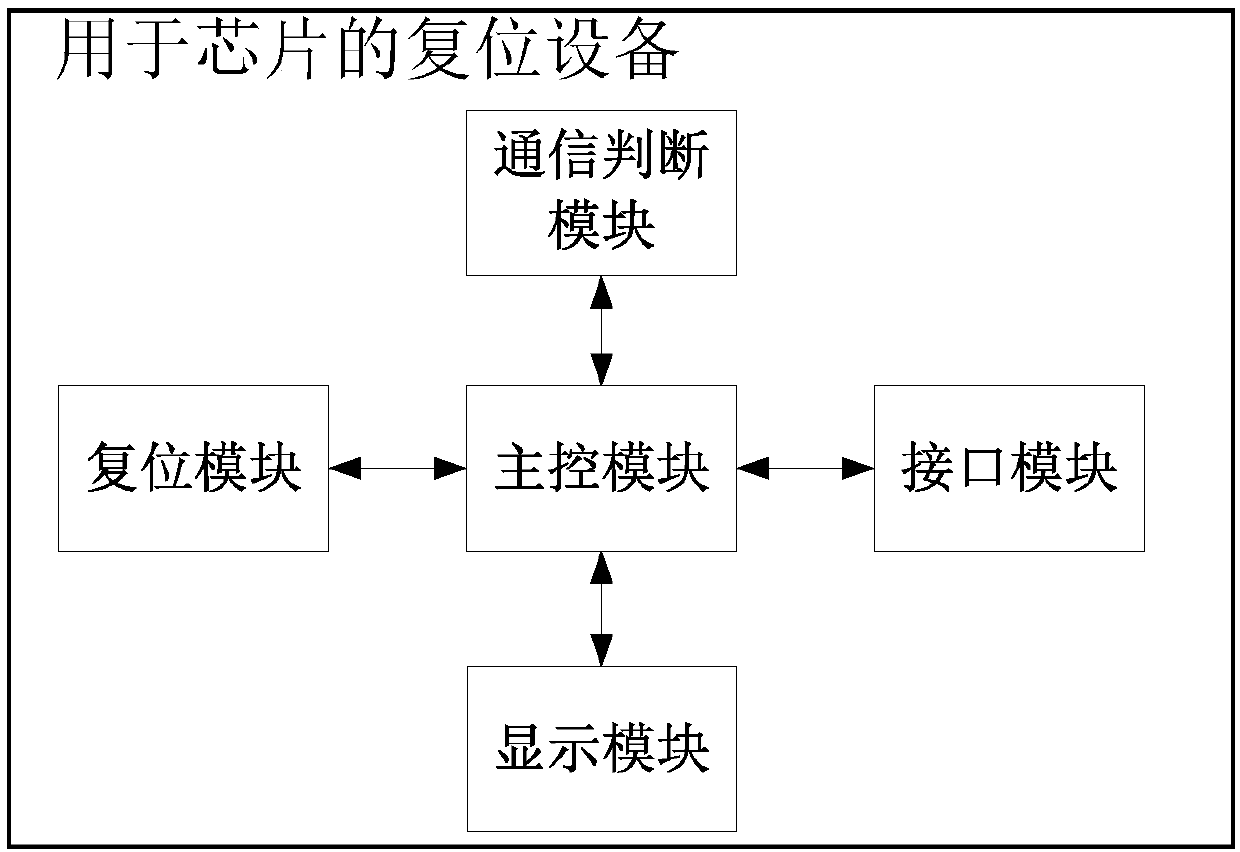
Reset method and equipment for chips, electronic equipment and storage medium
A reset method and chip technology, applied in the direction of digital output to the printing unit, etc., can solve the problems of different internal data reset methods, time-consuming, error-prone, etc., and achieve the effect of automatic selection, good compatibility, and low error rate.
- Summary
- Abstract
- Description
- Claims
- Application Information
AI Technical Summary
Problems solved by technology
Method used
Image

Examples
Embodiment Construction
[0031] Below, the present invention will be further described in conjunction with the accompanying drawings and specific implementation methods. It should be noted that, under the premise of not conflicting, the various embodiments described below or the technical features can be combined arbitrarily to form new embodiments. .
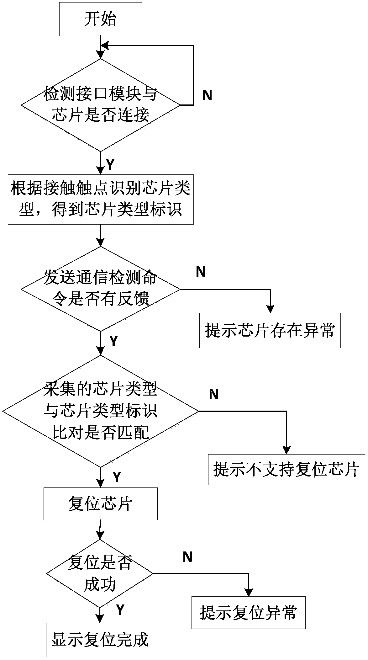
[0032] reset method for the chip, such as figure 1 shown, including the following steps:
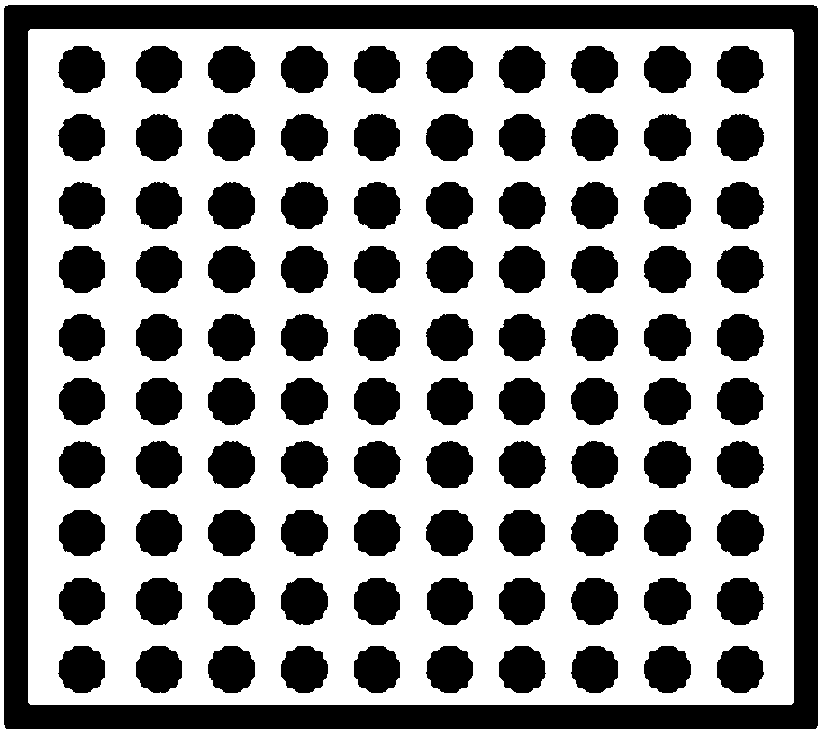
[0033] Chip type identification, identifying the contact between the probe matrix and the electrical connection point of the chip, obtaining the shape of the contact, judging the type of the chip according to the shape of the contact, and obtaining the chip type identification; preferably, identifying the contact between the probe matrix and the electrical connection point of the chip Specifically, the contact points are to sequentially increase the voltage value of the probes, collect the voltage values of other probes, record the coordinates of the probes th...
PUM
 Abstract
Description
Claims
Application Information
 - Generate Ideas
- Intellectual Property
- Life Sciences
- Materials
- Tech Scout
- Unparalleled Data Quality
- Higher Quality Content
- 60% Fewer Hallucinations
Browse by: Latest US Patents, China's latest patents, Technical Efficacy Thesaurus, Application Domain, Technology Topic, Popular Technical Reports.
© 2025 PatSnap. All rights reserved.Legal|Privacy policy|Modern Slavery Act Transparency Statement|Sitemap|About US| Contact US: help@patsnap.com