Solder mask hole-plugging structure and hole plugging method thereof

A technology of solder resist ink and hole plugging, which is applied in the direction of electrical connection formation of printed components, electrical connection of printed components, printed circuit components, etc., which can solve the problems of solder resist ink residue, shrinkage of confined space, gas expansion, etc., and achieve convenient processing , simple structure, and the effect of improving quality

Active Publication Date: 2018-01-16
DIGITAL PRINTED CIRCUIT BOARD CO LTD
View PDF8 Cites 5 Cited by
  • Summary
  • Abstract
  • Description
  • Claims
  • Application Information

AI Technical Summary

Problems solved by technology

[0003] The traditional plugging method is to set a backing plate at the bottom of the via hole on the PCB board, and stuff the solder resist ink into the via hole through the screen. A closed space is formed between the soldering ink and the backing plate. With the infiltration of the solder resist ink, the closed space is continuously reduced until the air pressure formed inside the closed space is equal to the sum of the external atmospheric pressure and the weight of the solder resist ink, and the solder resist ink can no longer Continue to plug into the via hole, resulting in insufficient solder resist ink plug hole saturation, and the plug hole effect is unsatisfactory; at the same time, gas expansion is prone to occur during baking, resulting in solder resist ink residue on the tin surface at the top of the via hole, Affects the performance of the tin surface on top of the via

Method used


Image

  • Solder mask hole-plugging structure and hole plugging method thereof

Examples


Embodiment Construction

[0022] In order to further understand the features, technical means, and specific objectives and functions achieved by the present invention, the present invention will be further described in detail below in conjunction with the accompanying drawings and specific embodiments.

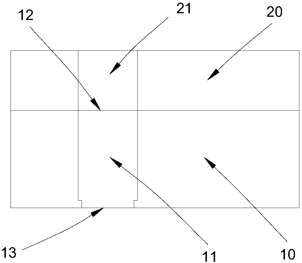
[0023] refer to figure 1 .

[0024] The embodiment of the present invention discloses a plug hole structure of solder resist ink, which includes a PCB substrate 10, an ink screen 20, and the ink screen 20 is located on the PCB substrate 10; the PCB substrate 10 includes a via hole 11, and one end of the via hole 11 is provided with S surface window 12, the other end of via hole 11 is provided with C surface window 13, S surface window 12 is positioned at an end near printing ink screen plate 20, is provided with mesh 21 in printing ink screen plate 20, via hole 11, S The axis center of the window 12 on the surface C, the window 13 on the C surface and the mesh 21 are the same; the diameter of the via ...


PUM


Abstract

The invention provides a solder mask hole-plugging structure and a hole plugging method thereof. The solder mask hole-plugging structure comprises a PCB substrate and a solder mask screen plate; the PCB substrate comprises a through hole; one end of the through hole is provided with an S-side open window, and the other end of the through hole is provided a C-side open window; a screen hole is formed in the screen plate; the diameter of the through hole is d; the diameter of the S-side open window is d; the diameter of the C-side open window ranges from 0.8d to 0.9d; the diameter of the screenhole is d; the screen hole is aligned with the S-side open window; the through hole is filled with solder mask from the S-side open window through the solder mask screen plate; and the PCB substrate is baked. With the solder mask hole-plugging structure and the hole plugging method thereof of the invention adopted, the solder mask can be effectively accommodated and borne; pressure of two ends ofthe solder mask can be effectively balanced, so that the solder mask can smoothly enter the through hole, and therefore, the saturation of the hole-plugging of the solder mask can be ensured; and thesolder mask will not be abnormally expanded due to pressure imbalance, so that it can be effectively ensured that the solder mask will not linger on the tin side of a PCB, and therefore, the quality of the hole-plugging of the PCB can be significantly improved.

Description

technical field [0001] The invention relates to a plug hole structure and a method, and specifically discloses a plug hole structure and a plug hole method of solder resist ink. Background technique [0002] With the advancement of science and technology, the structure and installation methods of electronic products are constantly updated, so the quality requirements for PCB boards are also getting higher and higher. At present, plugging operations are required during the production of PCB boards, and some via holes of the PCB board are filled with solder resist ink. The function of the plug hole is: in each via hole of the PCB board, except for the hole for installing electrical components, for the remaining via holes that do not need to be exposed, the solder resist ink can prevent flux or solder from passing through the solder surface during subsequent soldering. The via hole reaches the C surface, the C surface is the component surface, and the S surface is the pin weld...

Claims


Application Information

Patent Timeline
Patent Type & Authority Applications(China)
IPC IPC(8): H05K1/11H05K3/40
Inventor 张涛李贤万
Owner DIGITAL PRINTED CIRCUIT BOARD CO LTD
Why Eureka
Try Eureka