Optical detection device, system and method

A technology of optical detection and device pairing, applied in electromagnetic radiation induction, special data processing applications, instruments, etc., can solve problems such as poor information timeliness, omission of quantities, and recording errors, and achieve the effect of improving efficiency

Inactive Publication Date: 2018-01-19
台州市吉吉知识产权运营有限公司
View PDF8 Cites 4 Cited by
  • Summary
  • Abstract
  • Description
  • Claims
  • Application Information

AI Technical Summary

Problems solved by technology

[0005] 1. High cost: Each production line needs a special person to supervise the inspection log information of the optical inspection station in real time. Once an error is detected, the current error PCB board coding value is recorded according to the log information, resulting in a waste of labor
[0006] 2. Not in time: The inspectors cannot give real-time feedback to the designers of the PCB defects detected by the current optical inspection station, resulting in poor timeliness of information
[0007] 3. Error-prone: The inspectors record the current erroneous PCB board coding values ​​with the naked eye. Once the number is too large, it is easy to cause omissions and record errors.

Method used


Image

  • Optical detection device, system and method
  • Optical detection device, system and method
  • Optical detection device, system and method

Examples


Embodiment Construction

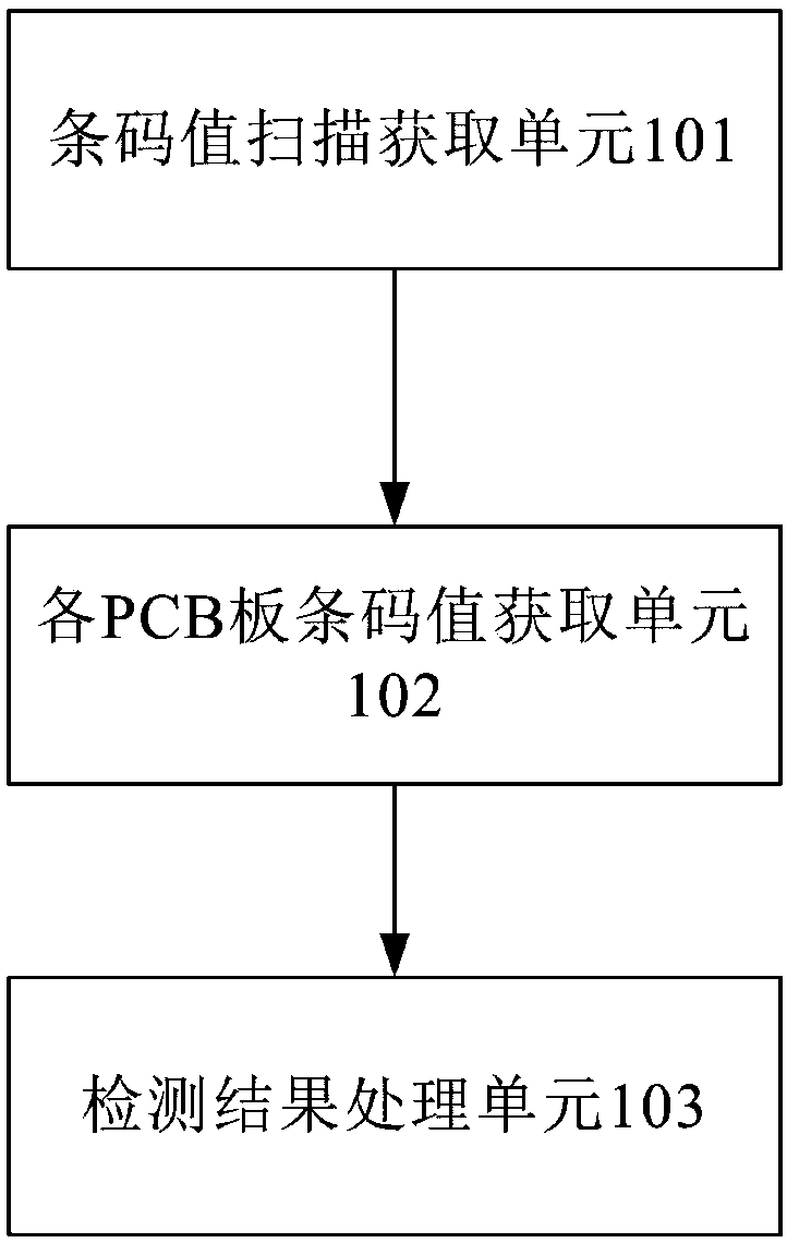
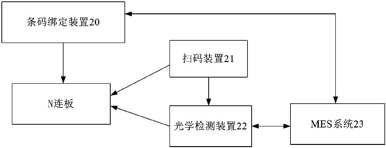
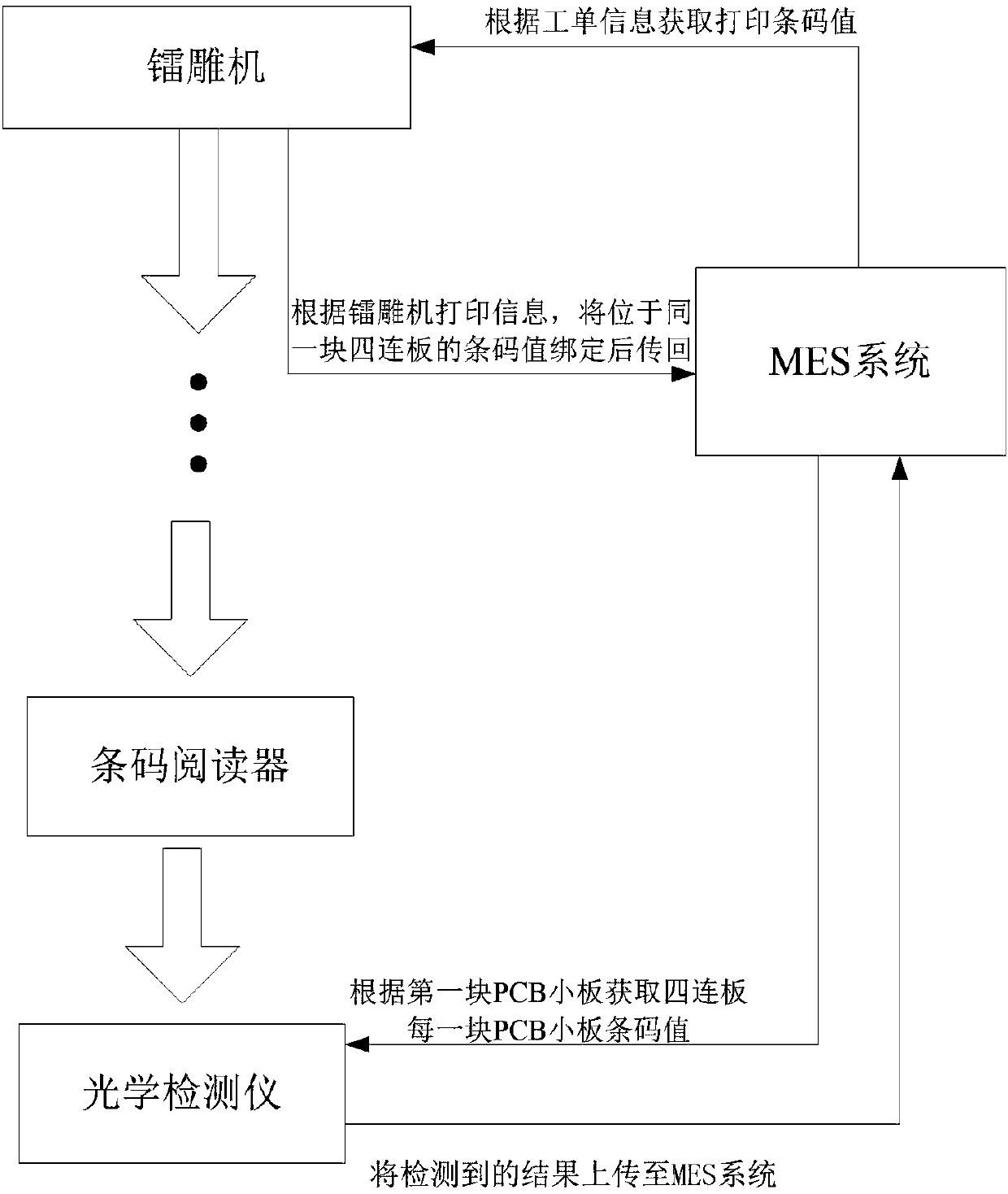
[0045] In order to more clearly illustrate the embodiments of the present invention or the technical solutions in the prior art, the specific implementation manners of the present invention will be described below with reference to the accompanying drawings. Obviously, the accompanying drawings in the following description are only some embodiments of the present invention, and those skilled in the art can obtain other accompanying drawings based on these drawings and obtain other implementations.

[0046] In order to make the drawing concise, each drawing only schematically shows the parts related to the present invention, and they do not represent the actual structure of the product. In addition, to make the drawings concise and easy to understand, in some drawings, only one of the components having the same structure or function is schematically shown, or only one of them is marked. Herein, "a" not only means "only one", but also means "more than one".

[0047] In one emb...


PUM


Abstract

The invention discloses an optical detection device, system and method. The optical detection device comprises a barcode value scanning and acquisition unit which is used for acquiring the barcode value of a certain small PCB of N connected boards; a barcode value acquisition unit of each PCB which is used for acquiring the barcode value of each small PCB of the N connected boards according to theacquired barcode value of the small PCB; and a detection result processing unit which is used for binding the detection result of each small PCB and the corresponding barcode value and performing uploading. With application of the optical detection device, system and method, the objective of real-time statistics of the circuit board optical detection result can be realized. The personnel for recording the information of wrong small PCB on each production line can be replaced so that the PCB design personnel are enabled to see the detection situation of the current AOI station in real time, and the efficiency of circuit board optical detection can be enhanced.

Description

technical field [0001] The invention relates to the technical field of PCBs, in particular to an optical detection device, system and method for counting optical detection results of circuit boards in real time. Background technique [0002] At present, in the production process of electronic products, for the production of PCB printed circuit boards, in order to reduce the cost of PCB production, four-connected boards, six-connected boards (hereinafter all take four-connected boards as an example) are generally used to splice multiple PCB single boards on way of producing together. However, in this way, it is difficult to directly locate small PCBs when the PCB is detected in the later stage. [0003] At present, the error statistics of the optical inspection station of the PCB board in the production process of electronic products are to obtain the relative position of the current error PCB small board in the four-connected board, write the information into the log, and t...

Claims


Application Information

Patent Timeline
Patent Type & Authority Applications(China)
IPC IPC(8): G06K7/14G06F17/50
Inventor 金通
Owner 台州市吉吉知识产权运营有限公司
Why Eureka
Try Eureka