Supercharge Your Innovation With Domain-Expert AI Agents!

A novel n-i-p-n half-mesa vertical silicon carbide avalanche diode and its preparation method

An n-i-p-n, silicon carbide avalanche technology, used in semiconductor devices, final product manufacturing, sustainable manufacturing/processing, etc., can solve the problems of poor p-type ohmic contact quality, large etching depth, low work efficiency, etc., to reduce extraction The number of wires, improving the cost performance of the device, and reducing the effect of etching damage

Active Publication Date: 2019-02-01
NANJING UNIV
View PDF4 Cites 0 Cited by
  • Summary
  • Abstract
  • Description
  • Claims
  • Application Information

AI Technical Summary

Problems solved by technology

[0007] In order to solve the problems of low working efficiency, large avalanche multiplication noise, and poor quality of p-type ohmic contact in traditional p-i-n type SiC APDs, as well as the need to use p-type silicon carbide substrates that are expensive and not yet commercialized in traditional n-i-p type SiC APDs, engraved In view of the problems of large etching depth, serious etching damage, large number of lead wires, and high manufacturing cost, the present invention provides a novel n-i-p-n half-mesa vertical structure silicon carbide avalanche diode and its preparation method

Method used


Image

  • A novel n-i-p-n half-mesa vertical silicon carbide avalanche diode and its preparation method
  • A novel n-i-p-n half-mesa vertical silicon carbide avalanche diode and its preparation method
  • A novel n-i-p-n half-mesa vertical silicon carbide avalanche diode and its preparation method

Examples


Embodiment 1

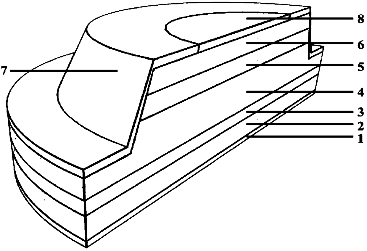
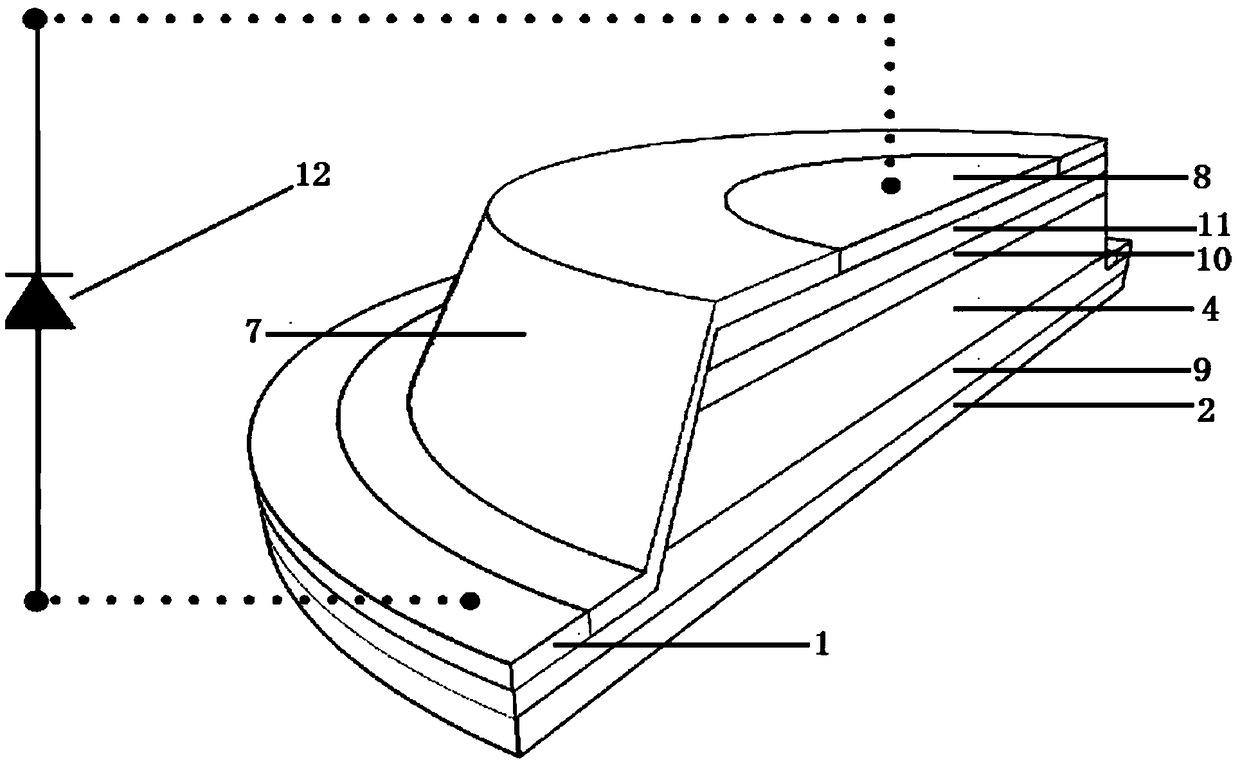
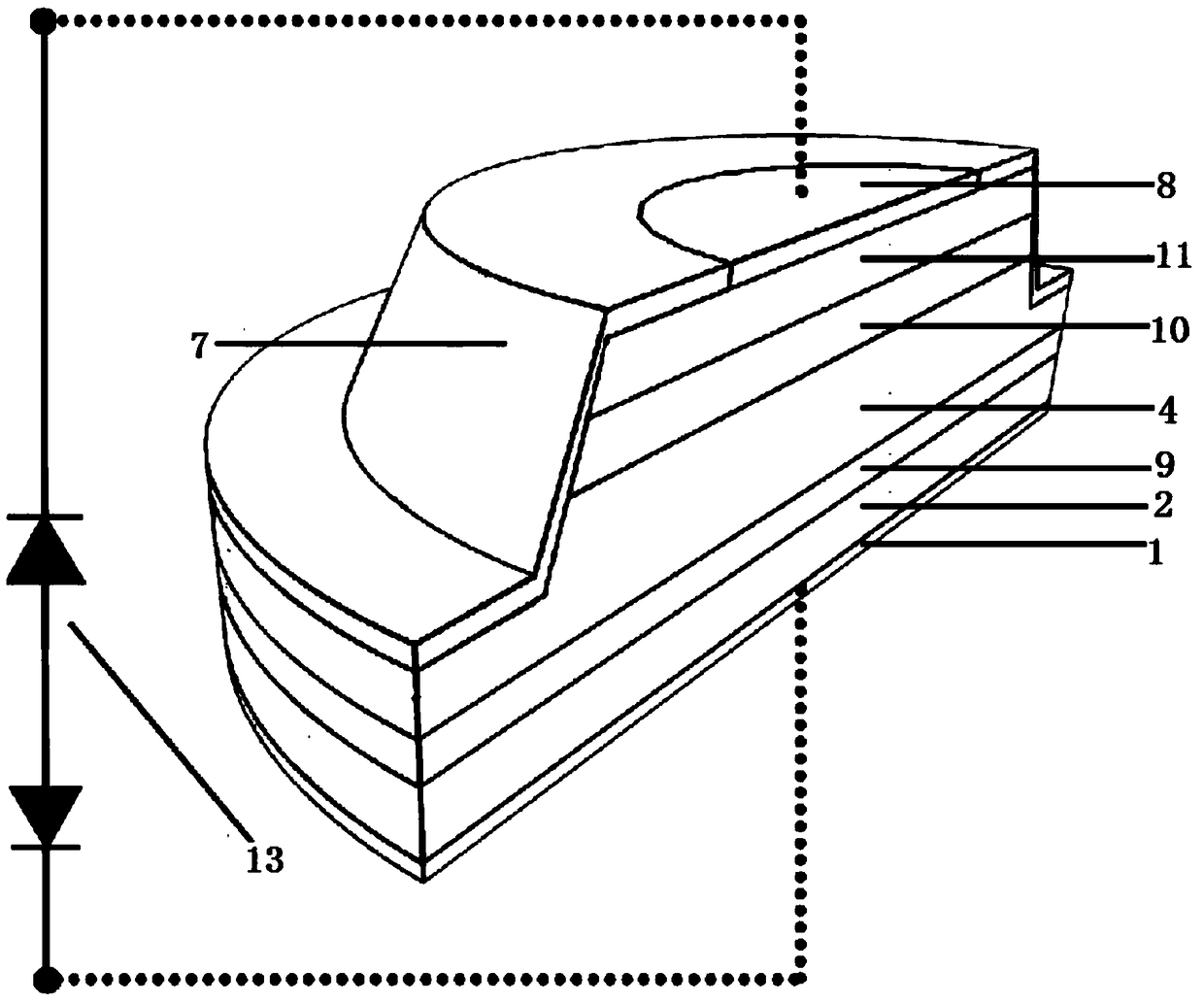
[0040] Such as image 3 As shown, using a novel n-i-p-n half-mesa vertical electrode structure, the device is fabricated on an n-type SiC substrate material. From the bottom to the top of the n-type SiC conductive substrate, there are p-type SiC transition layer, i-type SiC avalanche layer, n-type SiC transition layer, and n+ type SiC contact layer; the mesa only needs to be etched below the n-type transition layer, and the mesa The bottom is on the i-type SiC avalanche layer. The lower metal contact electrode is covered on the n-type SiC conductive substrate, and the upper metal contact electrode is on the n+ type SiC contact layer.

Embodiment 2

[0061] Basically the same as Embodiment 1, the difference is: the n-type contact electrode (lower metal contact electrode) and the p-type contact electrode (upper metal contact electrode) of the detector are all multilayer structures based on metal Ni and Au: Ni / Ti / Al / Au35 / 50 / 200 / 100nm, the Ni layer of the upper metal contact electrode is in contact with the n+ type SiC contact layer, and the Ni layer of the lower metal contact electrode is in contact with the n-type conductive SiC substrate. Compared with simple Ni / Au alloy electrodes, Ni / Ti / Al / Au composite electrodes have better ohmic contact quality, smaller specific contact resistance and lower reverse leakage current.


PUM

PropertyMeasurementUnit
thicknessaaaaaaaaaa
thicknessaaaaaaaaaa
thicknessaaaaaaaaaa

Abstract

The invention discloses a silicon carbide avalanche diode of a novel n-i-p-n half-mesa vertical structure and a preparation method thereof. According to the invention, the silicon carbide avalanche diode is of a n-i-p-n structure and sequentially comprises a lower metal contact electrode, an n-type conductive SiC substrate, a p-type SiC contact layer, an i-type SiC avalanche layer, an n-type SiC transition layer, an n+ type SiC contact layer and an upper metal contact electrode from bottom to top. The n-type SiC transition layer and the n+ type SiC contact layer form a mesa type large in bottom and small in top. The area of the lower surface of the n-type SiC transition layer is smaller than the area of the upper surface of the i-type SiC avalanche layer. A passivation layer is respectively arranged at the periphery of the n-type SiC transition layer, the periphery of the n+ type SiC contact layer and the upper surface of the i-type SiC avalanche layer which is not covered by the n-type SiC transition layer. According to the invention, the etching damage is reduced, so that the cost performance of the device is improved. The device can adopt n-type ohmic contact with better quality, so that the working efficiency of the device is improved. The avalanche noise is reduced, and the number of lead-out wires is reduced. The cost of the device is reduced.

Description

technical field [0001] The invention relates to a novel n-i-p-n half-mesa vertical structure silicon carbide avalanche diode and a preparation method thereof, belonging to the field of silicon carbide avalanche diodes. Background technique [0002] As one of the representatives of the third-generation wide bandgap semiconductors, silicon carbide (SiC) has excellent characteristics such as wide band gap, high breakdown field strength, high electron saturation velocity, high thermal conductivity, and good chemical stability. In recent years, with a large amount of research and development investment in SiC materials at home and abroad, the material quality and manufacturing process technology have been significantly improved, making it the preferred material for the preparation of high-power, high-temperature, and high-efficiency ultraviolet avalanche detector devices (APD). Among them, the 4H-SiC semiconductor material has a band gap of 3.26eV, which is the preferred material...

Claims


Application Information

Patent Timeline
Patent Type & Authority Patents(China)
IPC IPC(8): H01L31/028H01L31/0352H01L31/107H01L31/18
CPCY02P70/50
Inventor 陆海蔡小龙李良辉周东
Owner NANJING UNIV
Features
  • R&D
  • Intellectual Property
  • Life Sciences
  • Materials
  • Tech Scout
  • Unparalleled Data Quality
  • Higher Quality Content
  • 60% Fewer Hallucinations
Learn More