NMOS type GOA circuit and display panel

A liquid crystal display panel and circuit technology, applied to static indicators, digital memory information, instruments, etc., can solve problems such as poor flicker uniformity, achieve consistent feedthrough voltage, good flicker uniformity, and ensure delay conditions

Active Publication Date: 2018-02-23
WUHAN CHINA STAR OPTOELECTRONICS TECH CO LTD
View PDF7 Cites 23 Cited by
  • Summary
  • Abstract
  • Description
  • Claims
  • Application Information

AI Technical Summary

Problems solved by technology

The feedthrough voltage of the upper and lower parts of the NMOS display panel is inconsistent, which eventually leads to poor flicker uniformity of the upper and lower parts of the NMOS display panel

Method used


Image

  • NMOS type GOA circuit and display panel
  • NMOS type GOA circuit and display panel
  • NMOS type GOA circuit and display panel

Examples


Embodiment Construction

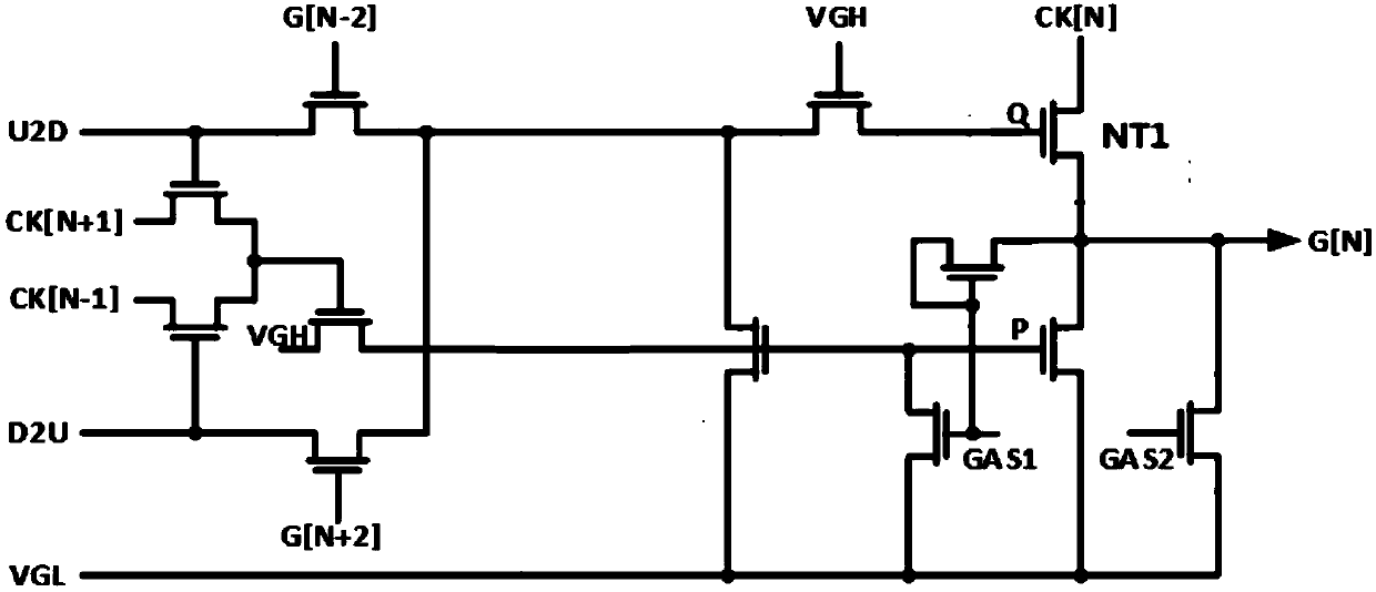
[0049] The present invention provides a kind of NMOS type GOA circuit, is used in liquid crystal display panel, such as Figure 4 As shown, in the first embodiment, the NMOS type GOA circuit includes M cascaded GOA units, and the Nth stage GOA unit includes: forward and reverse scanning control circuit 200, node signal control circuit 300, node signal output circuit 400 , pull-down circuit 500, and output circuit 100.

[0050] The forward and reverse scan control circuit 200 is used to control the GOA circuit to perform forward scan or reverse scan according to the forward scan control signal U2D or the reverse scan control signal D2U.

[0051] The output circuit 100 includes a first TFT NT1 and a second TFT NT2, the node signal output circuit 400 includes a third TFT NT3, and the pull-down circuit 500 includes a fourth TFT NT4.

[0052] The first end of the second thin film transistor NT2 is connected to the high potential signal VGH, the second end of the second thin film t...


PUM


Abstract

The invention provides an NMOS type GOA circuit and a display panel. The circuit comprises M cascaded GOA units, wherein an output circuit of the Nth stage of GOA unit comprises a first thin-film transistor and a second thin-film transistor, a node signal output circuit comprises a third thin-film transistor, and a pull-down circuit comprises a fourth thin-film transistor; a high-potential signalaccesses into a first end of the second thin-film transistor or the first end of the second thin-film transistor is connected with a third end of the first thin-film transistor, a second end of the second thin-film transistor is connected with a first end of the first thin-film transistor, and an Nth clock signal accesses into a third end of the second thin-film transistor; the third end of the first thin-film transistor is connected with the output end of a forward and reverse scanning control circuit, a low-potential signal accesses into the third end of the first thin-film transistor through a first voltage-stabilizing capacitor, and a second end of the first thin-film transistor is connected with a first end of the fourth thin-film transistor and serves as the output end of an Nth stage of grid driving signal. For the NMOS type GOA circuit and the display panel, the feeding-through voltage of an AA area of the display panel is enabled to be consistent, and the display panel has good flickering uniformity.

Description

technical field [0001] The invention relates to the field of display technology, in particular to an NMOS type GOA circuit and a display panel. Background technique [0002] The GOA (Gate Driver on Array, array substrate row driving technology) circuit is a circuit that realizes the progressive scanning of the display panel. Now the commonly used driving circuits in the display panel include CMOS-type GOA circuits and NMOS-type GOA circuits. The CMOS-type GOA circuits include NTFT (N-channel thin film transistor) devices and PTFT (P-channel thin film transistor) devices; and only NTFT devices are included in the NMOS type GOA circuit. Now the GOA control signal line in the NMOS display panel is directly connected to the first-level GOA unit through the WOA wiring, and the GOA control signal line needs to pass through a large RC circuit (Resistance-Capacitance Circuits, that is, a phase shift circuit, or RC filter. , RC network) to access the last level of GOA unit. In this...

Claims


Application Information

Patent Timeline
Patent Type & Authority Applications(China)
IPC IPC(8): G09G3/36
CPCG09G3/3674G11C19/28G09G3/20G09G2300/0408G09G2310/0267G09G2310/0286G09G2320/0247G09G3/3677G09G2310/0202G09G2310/0283G09G2320/0219G11C19/184G11C19/00
Inventor 洪光辉
Owner WUHAN CHINA STAR OPTOELECTRONICS TECH CO LTD
Why Eureka
Try Eureka