Lateral double diffused metal oxide semiconductor device

An oxide semiconductor and lateral double diffusion technology, applied in semiconductor devices, electrical components, circuits, etc., can solve the problem that the breakdown voltage cannot be further increased, and achieve the effect of reducing the length, increasing the breakdown voltage, and reducing the electric field

Active Publication Date: 2020-09-04
NUVOTON
View PDF4 Cites 0 Cited by
  • Summary
  • Abstract
  • Description
  • Claims
  • Application Information

AI Technical Summary

Problems solved by technology

[0005] However, traditional LDMOS transistors have high turn-on resistance due to the limitation of the length of the drift region, and the breakdown voltage cannot be further increased

Method used


Image

  • Lateral double diffused metal oxide semiconductor device
  • Lateral double diffused metal oxide semiconductor device
  • Lateral double diffused metal oxide semiconductor device

Examples


Embodiment Construction

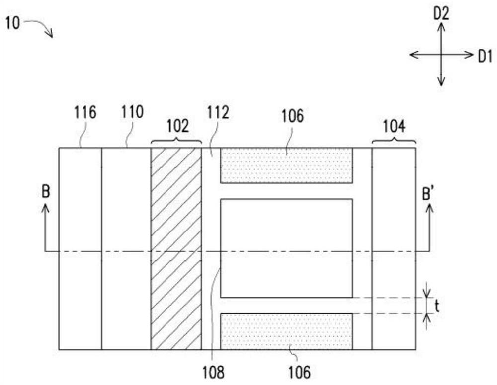
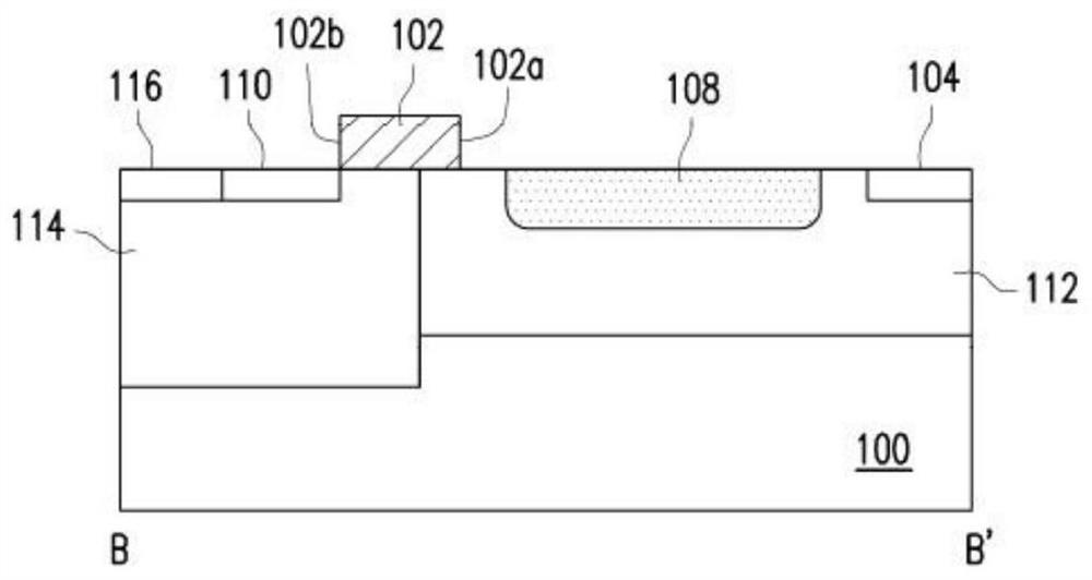
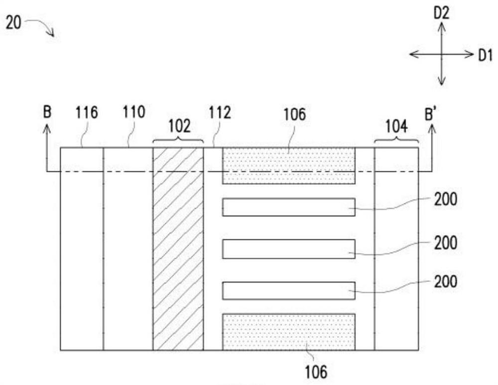
[0049] The drawings attached to the following embodiments are intended to more fully describe the exemplary embodiments of the inventive concept. However, many different forms can be used to implement the present invention, and the present invention should not be regarded as limited to the description. 的实施例。 Example. In the drawings attached to the present invention, for clarity, the sizes and relative sizes of the layers and regions may be exaggerated.

[0050] In the following, the first conductivity state is n-type and the second conductivity state is p-type as an example for description, but the present invention is not limited to this. Those with ordinary knowledge in the technical field to which the present invention pertains should understand that the first conductivity state can also be replaced with p-type and the second conductivity state can be replaced with n-type. Among them, the n-type dopant is, for example, phosphorus or arsenic; the p-type dopant is, for example,...


PUM


Abstract

A lateral double-diffused metal oxide semiconductor element includes: a substrate, a gate structure, a drain region, a plurality of isolation structures, at least one doping region and a source region. The gate structure is on the substrate. The drain region and the source region are respectively located in the substrate on the first side and the second side of the gate structure. Both the isolation structure and the doping region are located in the substrate between the gate structure and the drain region, wherein the extension direction of the isolation structure is different from that of the gate structure. The doped region can be located between two isolation structures or under the isolation structure, wherein the doped region and the drain region have opposite conductivity states, so that the turn-on resistance of the lateral double-diffused metal oxide semiconductor device is reduced, and the gate structure and The electric field between the drain regions increases the breakdown voltage of the lateral double-diffused metal oxide semiconductor device.

Description

Technical field [0001] The present invention relates to a semiconductor device, and more particularly to a lateral double-diffused metal oxide semiconductor (LDMOS) device. Background technique [0002] In recent years, power semiconductor devices have been used in various semiconductor industries. Power semiconductor components include high-voltage integrated circuits, which typically include one high-voltage transistor or multiple high-voltage transistors usually on the same silicon chip as a low-voltage circuit. Among the above-mentioned integrated circuits, the most commonly used high-voltage components are lateral double diffused metal oxide semiconductor (LDMOS) transistors. In high-voltage integrated circuits, LDMOS structures can usually be manufactured by using some of the same techniques used to manufacture low-voltage circuits and logic circuits. Generally speaking, the current LDMOS structure is fabricated in a thick epitaxial layer with the conductivity state oppos...

Claims


Application Information

Patent Timeline
Patent Type & Authority Patents(China)
IPC IPC(8): H01L29/06H01L29/78
CPCH01L29/0634H01L29/7816H01L29/7835H01L29/0653H01L29/0692
Inventor 许健杨绍明钱德拉·谢卡尔阿南德赛义德·萨瓦尔·以曼
Owner NUVOTON
Why Eureka
Try Eureka