
Junction field-effect transistor (JFET) pipe compatible process with double pole and P-ditch aligning automatically

A self-alignment and process technology, applied in electrical components, semiconductor/solid-state device manufacturing, circuits, etc., can solve problems such as large parasitic capacitance and large manufacturing process deviation, and achieve large dynamic resistance, good consistency, offset and leakage. The effect of low current

Active Publication Date: 2013-02-06
EAST CHINA INST OF OPTOELECTRONICS INTEGRATEDDEVICE
View PDF2 Cites 1 Cited by
  • Summary
  • Abstract
  • Description
  • Claims
  • Application Information

AI Technical Summary

Problems solved by technology

[0003] The purpose of the present invention is to solve the defects of large gate-source / drain overlapping parasitic capacitance and large manufacturing process deviation formed by the existing non-self-aligned gate, and provide a P-channel with a bipolar circuit and gate self-aligned structure JEFT tube compatible process

Method used


Image

  • Junction field-effect transistor (JFET) pipe compatible process with double pole and P-ditch aligning automatically
  • Junction field-effect transistor (JFET) pipe compatible process with double pole and P-ditch aligning automatically
  • Junction field-effect transistor (JFET) pipe compatible process with double pole and P-ditch aligning automatically

Examples


Embodiment Construction

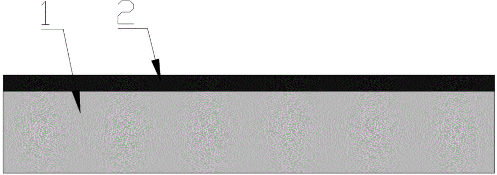
[0041] First, the substrate is selected as a P-type 4-inch silicon wafer, with a resistivity of (8-13) Ω.cm and a thickness of (525±20) μm; then the substrate is cleaned: the silicon wafer needs to be chemically cleaned, The cleaning chemicals are concentrated sulfuric acid, hydrogen peroxide and hydrofluoric acid. Concentrated sulfuric acid and hydrogen peroxide are strong oxidants that can remove particles or dust on the surface of silicon wafers. In the process of boiling concentrated sulfuric acid, a natural oxide layer will be formed on the surface of the silicon wafer, which needs to be rinsed with hydrofluoric acid, rinsed with high-purity deionized water, and centrifugally dried under nitrogen protection.

[0042] Proportion of chemical reagents and ambient temperature:

[0043] Sulfuric acid:hydrogen peroxide=3:1 temperature is (115±5)℃

[0044] Hydrofluoric acid: water = 1:30 temperature is room temperature

[0045] Deionized water resistivity ≥ 18MΩ.cm.

[0046] ...


PUM

PropertyMeasurementUnit
Resistanceaaaaaaaaaa

Abstract

The invention relates to a junction field-effect transistor (JFET) pipe compatible process with a double pole and a P-ditch aligning automatically. By means of grid region pre-oxidation, ditch region boron filling, grid region phosphorus filling and the annealing process, a method for manufacturing a double pole and grid self-aligning P-ditch JEFT compatible integrated amplifier is achieved. By means of the JEFT pipe compatible process, the shortcomings that a grid source / leakage overlapping parasitic capacitance formed by the existing non-self-aligning grid is large, a source end resistor and the drift region length are both large, and the device depends on graph dimension and dosage concentration of the ditch region and the drift region are overcome. The P-ditch JFET pipe process with the grid aligning automatically has the advantages of achieving self aligning of the grid region and the source / leak region, and reducing the drift region length of the grid source / leak overlapping parasitic capacitance and the source end resistance and the leakage end; and the P-ditch JEFT pipe is large in output dynamic resistance and, good in consistency of transconductance and punch-off voltage, and small in detuning and leakage current.

Description

technical field [0001] The invention belongs to the field of semiconductor technology manufacturing, and in particular relates to a bipolar circuit and a P-channel JEFT tube compatible technology with a grid self-alignment structure. Background technique [0002] The gate-source / drain overlap parasitic capacitance formed by the non-self-aligned gate of the bipolar and P-channel self-aligned JFET is large, the source resistance and the length of the drift region are too large, and the device depends on the pattern of the channel region and the drift region size and doping concentration. One end of the non-self-aligned gate drift region and the gate will have some process deviations (such as photolithography CD, overlapping, etch CD, etc.), which can affect the channel length of the device, mainly affected by the photolithography process and equipment. . Contents of the invention [0003] The purpose of the present invention is to solve the defects of large gate-source / dra...

Claims


Application Information

Patent Timeline
IPC IPC(8): H01L21/8248
Inventor 丁继洪吕东锋陈计学李苏苏简崇玺
Owner EAST CHINA INST OF OPTOELECTRONICS INTEGRATEDDEVICE
Learn More