Method for fabricating radio frequency ldmos devices with double metal silicides

A manufacturing method and silicide technology, applied in semiconductor/solid-state device manufacturing, semiconductor devices, electrical components, etc., can solve problems such as large sheet resistance and leakage, and achieve high output power, easy integration, and simple process flow. Effect

Active Publication Date: 2015-10-14
SHANGHAI HUAHONG GRACE SEMICON MFG CORP
View PDF6 Cites 0 Cited by
  • Summary
  • Abstract
  • Description
  • Claims
  • Application Information

AI Technical Summary

Problems solved by technology

In order to minimize the gate resistance, a thicker metal silicide thickness is required, but using the same metal silicide on the source and drain will cause leakage into the monocrystalline silicon layer and penetrate the junction.
An existing compromise is to stack tungsten-silicon alloy on heavily doped polysilicon as the gate, and use conventional titanium metal silicide to form the source and drain, but the sheet resistance of this structure is still very large

Method used


Image

  • Method for fabricating radio frequency ldmos devices with double metal silicides
  • Method for fabricating radio frequency ldmos devices with double metal silicides
  • Method for fabricating radio frequency ldmos devices with double metal silicides

Examples


Embodiment Construction

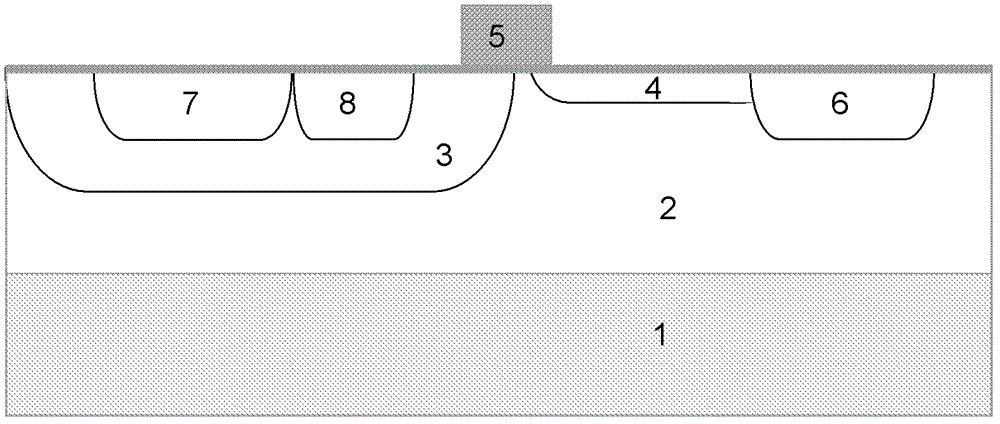
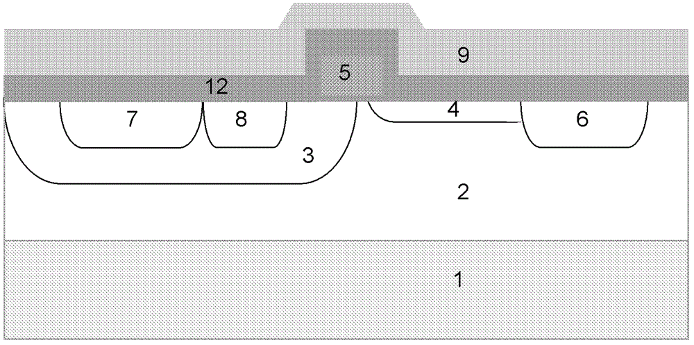
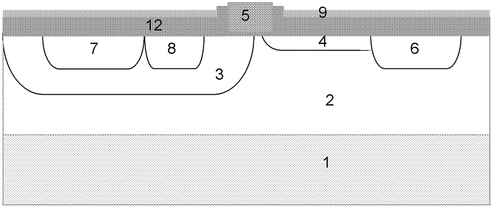
[0023] The manufacturing method of the radio frequency LDMOS device with double metal silicide of the present invention comprises the following steps:

[0024] The first step is to grow a low-doped P-type epitaxy 2 on a heavily doped P-type silicon substrate 1, grow a gate oxide layer on the P-type epitaxy 2, and deposit polysilicon on the gate oxide layer. etch to form polysilicon gate 5, and the doping concentration of P-type epitaxy 2 is 10 14 ~10 16 cm -3 ;

[0025] In the second step, ion implantation is performed on the self-aligned polysilicon gate in the P-type epitaxy 2, and a P well 3 is formed through high temperature advancement. One end of the P well 3 is located under the polysilicon gate 5;

[0026] The third step is to perform ion implantation to form N-type heavily doped source region 8 and P-type heavily doped lead-out region 7 in P well 3, and form N-type low-doped drain region 4 and N-type drain region 4 in P-type epitaxy 2. Type heavily doped drain reg...


PUM


Abstract

The invention discloses a radio frequency laterally diffused metal oxide semiconductor (LDMOS) device with thermometal silicide and a manufacturing method. A P-shaped silicon substrate is provided with P-shaped epitaxy. A N-shaped low doped drain region, a P trap and a N-shaped heavy doped drain region are arranged in the P-shaped epitaxy. A N-shaped heavy doped source region and a P-shaped heavy doped lead out region are arranged in the P trap. A drain electrode titanium silicide layer is arranged on the top of the N-shaped heavy doped source region. A source electrode titanium silicide layer is arranged on the top of the P-shaped heavy doped lead out region and the N-shaped heavy doped source region. A grid electrode titanium silicide layer is arranged on the top of a polycrystalline silicon grid electrode. Thickness of the grid electrode titanium silicide layer is larger than thickness of the drain electrode titanium silicide layer and the source electrode titanium silicide layer. Titanium silicide of a grid electrode is thicker, square resistance of the grid electrode is reduced, and normal thickness titanium silicide on a source electrode and a source electrode avoids electricity leakage to caused by junction penetration of source drain and the trap.

Description

technical field [0001] The invention relates to the field of semiconductor integrated circuits, in particular to a method for manufacturing an RFLDMOS thick isolation dielectric layer structure. Background technique [0002] In high-speed RF LDMOS, the gate resistance is an important factor affecting the switching speed of the device. Since this device requires high output power, the total width will be very large, and multiple fingers are required, and the width of a single finger, that is, the gate length, is also very long, which inevitably makes the series resistance large and needs to be reduced. The square resistance of the gate, and the source and drain also need lower resistance. To minimize the gate resistance, a thicker metal silicide thickness is required, but using the same metal silicide on the source and drain will lead to deeper penetration into the monocrystalline silicon layer and penetration of the junction causing leakage. An existing compromise is to st...

Claims


Application Information

Patent Timeline
Patent Type & Authority Patents(China)
IPC IPC(8): H01L29/41H01L29/78H01L21/28H01L21/336
CPCH01L29/7835H01L29/1045
Inventor 周正良遇寒
Owner SHANGHAI HUAHONG GRACE SEMICON MFG CORP
Why Eureka
Try Eureka