Silicon carbide semiconductor element and manufacturing method thereof

a silicon carbide and semiconductor element technology, applied in the field of semiconductor elements, can solve the problems of uneven thickness of the gate oxide layer, high electric field crowded, sic damage, etc., and achieve the effect of reducing the turn-on resistance of mos-controlled elements and enhancing element reliability

Active Publication Date: 2018-07-10
SHANGHAI HESTIA POWER INC
View PDF4 Cites 3 Cited by
  • Summary
  • Abstract
  • Description
  • Claims
  • Application Information

AI Technical Summary

Benefits of technology

[0027]In conclusion, compared to the prior art, the present invention achieves following effects. By spacing the first doped region from the surface of the semiconductor layer by the first depth, and disposing the shallow doped region between the first doped region and the surface of the semiconductor layer, the turn-on resistance of a MOS controlled element can be reduced while a predetermined threshold voltage can be maintained. Further, as the surface of the semiconductor layer is not doped with a high concentration, the variation in thickness of gate dielectric layer due to concentration dependent oxidation of SiC can be avoided. Thus, element reliability can be enhanced.

Problems solved by technology

While the gate oxide layer is grown, the high-concentration n-type doped region has a faster oxidation rate than that of a p-type well, hence resulting in an uneven thickness of the gate oxide layer.
Further, during the process of forming high doping concentration source region, a part of lattices of SiC may be damaged due to collisions with implanted ions to transform into amorphous structures.
As a result, a high electric field may be crowded around some localized points of gate oxide, and poses reliability concerns.
In addition, during the thermal oxidation of SiC, the unreacted carbon will remain at the interface and inside of oxide as defects in the form of silicon vacancies, carbon clusters and carbon interstitials, and create energy states in the band gap.
In the meantime the acceptor-like traps filled with electrons will become negatively charged, and cause significant Coulomb scattering of electrons.
However, the current approaches of reducing on-resistance usually face the trade-off of lowered MOSFET threshold voltage.
A low threshold voltage increases the risk of falsely turn-on during operation of devices

Method used


Image

  • Silicon carbide semiconductor element and manufacturing method thereof
  • Silicon carbide semiconductor element and manufacturing method thereof
  • Silicon carbide semiconductor element and manufacturing method thereof

Examples


Embodiment Construction

[0036]Details and technical contents of the present invention are given with the accompanying drawings below.

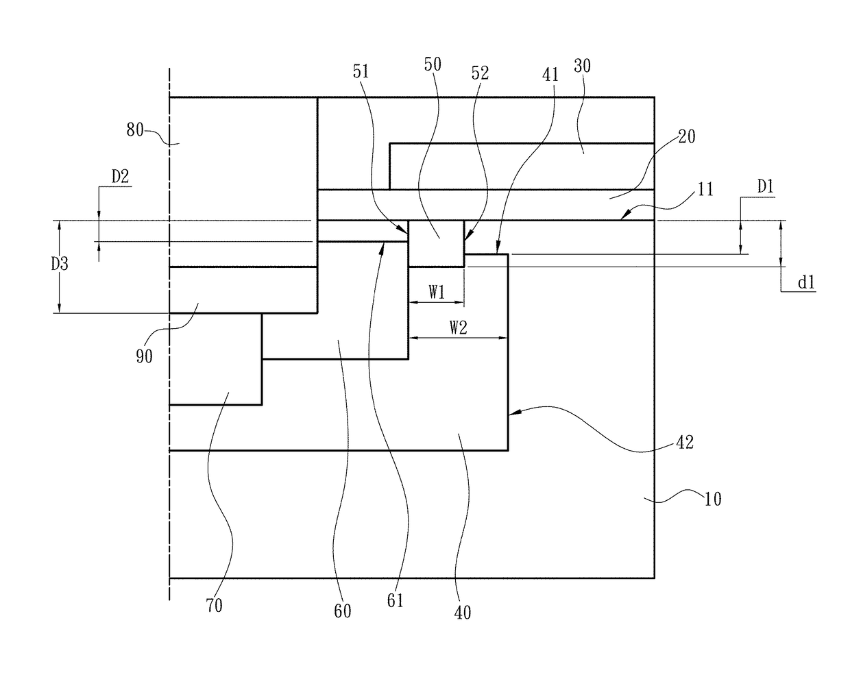
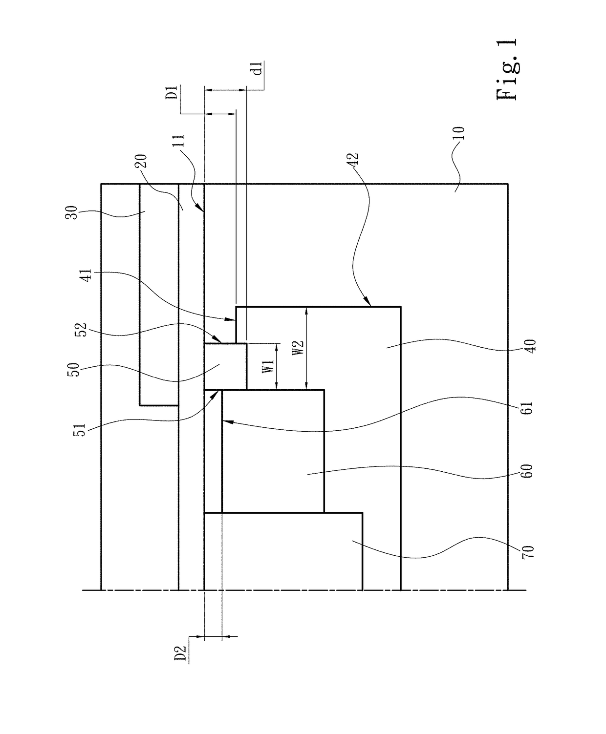
[0037]FIG. 1 and FIG. 2 are a section view before a source electrode is formed and a section view after the source electrode is formed, respectively. As shown, a silicon carbide (SiC) semiconductor element provided by the present invention includes a semiconductor layer 10, a dielectric layer 20, a gate electrode layer 30, a first doped region 40, a shallow doped region 50, a second doped region 60 and a third doped region 70. The semiconductor layer 10 is of a first conductivity type and includes a surface 11. The dielectric layer 20 is on the surface 11 of the semiconductor layer 10. The gate electrode layer 30 is on the dielectric layer 20. In the embodiment, the first conductivity type is n type. In the present invention, the semiconductor layer 10 is made of 4H—SiC, and has a thickness between 1 μm and 35 μm and a doping concentration between 1×1014 cm−3 and 1×1017 cm−3....


PUM


Abstract

A silicon carbide (SiC) semiconductor element includes a semiconductor layer, a dielectric layer on a surface of the semiconductor layer, a gate electrode layer on the dielectric layer, a first doped region, a second doped region, a shallow doped region and a third doped region. The semiconductor layer is of a first conductivity type. The first doped region is of a second conductivity type and includes an upper doping boundary spaced from the surface by a first depth. The shallow doped region is of the second conductivity type, and extends from the surface to a shallow doped depth. The second doped region is adjacent to the shallow doped region and is at least partially in the first doped region. The third doped region is of the second conductivity type and at least partially overlaps the first doped region.

Description

FIELD OF THE INVENTION[0001]The present invention relates to a semiconductor element, and particularly to a silicon carbide (SiC) semiconductor element.BACKGROUND OF THE INVENTION[0002]Semiconductor power devices, in terms of blocking voltage in design, should provide characteristics of minimum conduction resistance, lower reverse leakage current and faster switching speed to reduce conduction loss and switching loss during operation. Silicon carbide (SiC) has characteristics of a wide energy bandgap (for instance, energy bandgap of 4H—SiC is 3.26 eV, compared to 1.1 eV of silicon), a higher critical field of dielectric breakdown (2.2 MV / cm) and a higher thermal conduction coefficient (4.9 W / cm-K), hence is deemed an excellent material for making power switching devices. Silicon carbide is also the only compound semiconductor can form thermally grown oxides, hence is suitable for manufacturing MOS controlled switches such as MOSFET (metal oxide semiconductor field effect transistor)...

Claims


Application Information

Patent Timeline
Patent Type & Authority Patents(United States)
IPC IPC(8): H01L29/16H01L29/78H01L29/10H01L29/08H01L29/417H01L29/66H01L21/04H01L29/739H01L29/04
CPCH01L29/1608H01L21/047H01L29/0865H01L29/1095H01L29/7393H01L29/7396H01L29/7802H01L29/7816H01L29/66068H01L29/41766H01L29/1045H01L29/45H01L21/26586
Inventor YEN, CHENG-TYNGHUNG, CHIEN-CHUNGHUNG, HSIANG-TINGHUANG, YAO-FENGLEE, CHWAN-YING
Owner SHANGHAI HESTIA POWER INC
Why Eureka
Try Eureka