Semiconductor device and manufacturing method thereof, and electronic device

A manufacturing method and semiconductor technology, applied in semiconductor/solid-state device manufacturing, semiconductor devices, circuits, etc., can solve the problems of reducing device performance, increasing device size, and large pitch size, so as to improve overall performance and integration, reduce Effect of turning on resistance and reducing pitch size

Inactive Publication Date: 2018-06-05
SEMICON MFG INT (SHANGHAI) CORP +1
View PDF4 Cites 2 Cited by
  • Summary
  • Abstract
  • Description
  • Claims
  • Application Information

AI Technical Summary

Problems solved by technology

[0005] Among them, such as figure 1 As shown in the traditional fully isolated LDMOS device with a body region, the body region is used to completely isolate adjacent LDMOS devices, and the critical dimension of the body region (the gap between the gate structure 101 and the gate structure 102 of the corresponding adjacent LDMOS device is critical Size) is large, and the ion implantation in the body region will not have a photoresist shielding (shielding) effect. Therefore, the pitch size between LDMOS devices is relatively large, increasing the size of the device is not conducive to the reduction of device integration, and the turn-on resistance ( Ron) is large, which reduces the performance of the device

Method used


Image

  • Semiconductor device and manufacturing method thereof, and electronic device
  • Semiconductor device and manufacturing method thereof, and electronic device
  • Semiconductor device and manufacturing method thereof, and electronic device

Examples


Embodiment 1

[0062] In order to solve the foregoing technical problems, the present invention provides a semiconductor device, which mainly includes:

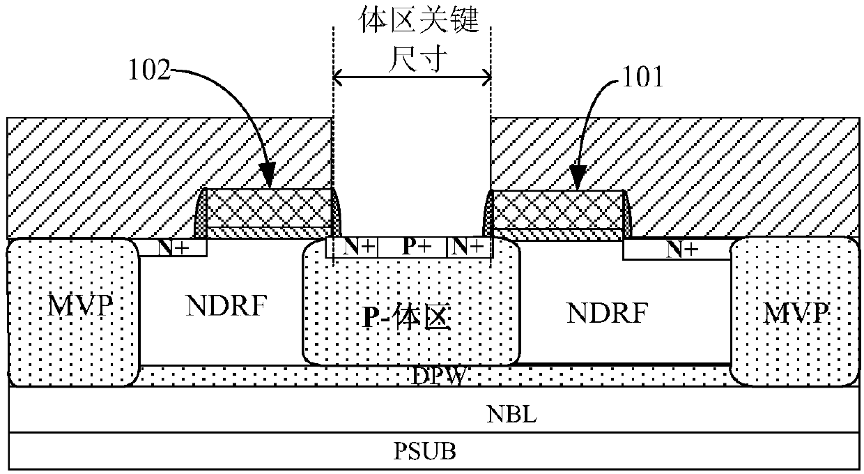
[0063] a semiconductor substrate having a first conductivity type, the semiconductor substrate comprising a first surface and a second surface opposite the first surface;

[0064] a body region with a first conductivity type formed in the semiconductor substrate, the body region includes a first portion and a second portion above and adjacent to the first portion, wherein the second portion is adjacent to the a first surface of a semiconductor substrate, the first portion extends along a first direction with a first width, the second portion extends along the first direction with a second width, and the first width is smaller than the second width;

[0065] a first gate structure disposed on the first surface of the semiconductor substrate and partially extending to the body region;

[0066] The second gate structure is disposed on the fir...

Embodiment 2

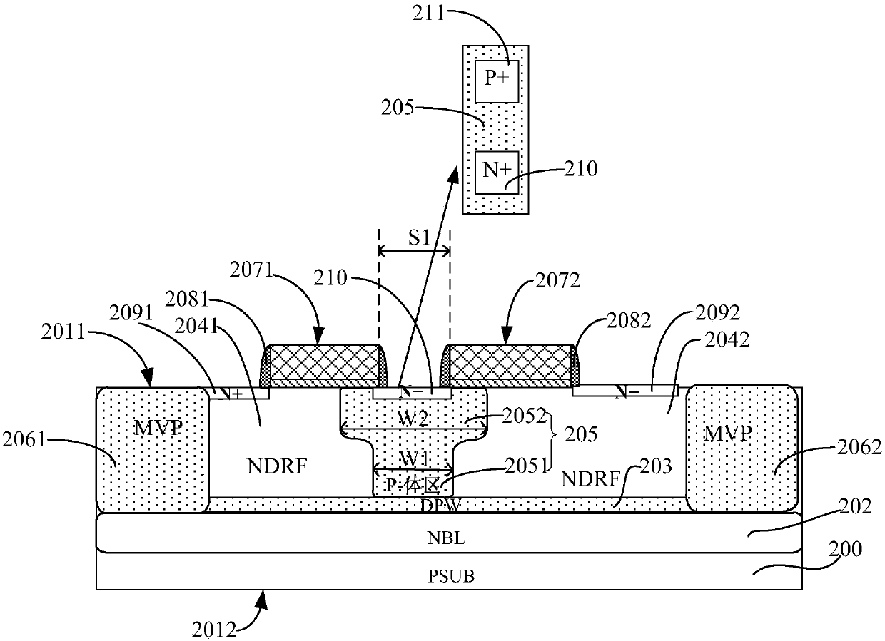
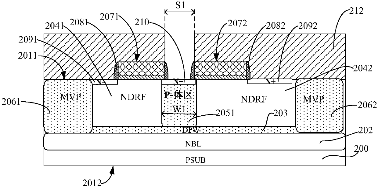
[0100] This implementation also provides a method for manufacturing a semiconductor device in the aforementioned implementation one, such as Figure 4 As shown, it mainly includes the following steps:

[0101] Step S1, providing a semiconductor substrate having a first conductivity type, the semiconductor substrate comprising a first surface and a second surface opposite to the first surface, and forming on the first surface of the semiconductor substrate a first gate structure and a second gate structure arranged at intervals along the first direction;

[0102] Step S2, forming a patterned mask layer with an opening to cover the first surface of the semiconductor substrate, wherein the opening exposes the gap between the first gate structure and the second gate structure said semiconductor substrate at the gap;

[0103] Step S3, performing a first ion implantation to form a first part of a body region in the semiconductor substrate exposed in the opening, wherein the first ...

Embodiment 3

[0161] The present invention also provides an electronic device, including the semiconductor device described in Embodiment 1, and the semiconductor device is prepared according to the method described in Embodiment 2.

[0162] The electronic device of this embodiment can be any electronic device such as a mobile phone, a tablet computer, a notebook computer, a netbook, a game console, a TV set, a VCD, a DVD, a navigator, a digital photo frame, a camera, a video camera, a recording pen, MP3, MP4, PSP, etc. Product or equipment, but also any intermediate product including electrical circuits. The electronic device according to the embodiment of the present invention has better performance due to the use of the above-mentioned semiconductor device.

[0163] in, Figure 5 An example of a mobile phone handset is shown. A mobile phone handset 500 is provided with a display portion 502 included in a casing 501, operation buttons 503, an external connection port 504, a speaker 505,...


PUM


Abstract

The invention provides a semiconductor device, a manufacturing method thereof and an electronic device, which relate to the technical field of semiconductors. The semiconductor device comprises a semiconductor substrate having a first conduction type, a body region having a first conduction type, a first gate structure and a second gate structure, wherein the body region is formed in the semiconductor substrate, the body region comprises a first portion and a second portion which is positioned on and adjacent to the first portion, the second portion is close to the first surface of the semiconductor substrate, the first portion extends for a first width along a first direction, the second portion extends for a second width along the first direction, and the first width is less than the second width; the first gate structure is arranged on the first surface of the semiconductor substrate, and partially extends onto the body region; and the second gate structure is arranged on the firstsurface of the semiconductor substrate, partially extends onto the body region, and is arranged along the first direction in a manner of being spaced from the first gate structure.

Description

technical field [0001] The present invention relates to the technical field of semiconductors, in particular to a semiconductor device, a manufacturing method thereof, and an electronic device. Background technique [0002] With the rapid development of the semiconductor industry, PIC (Power Integrated Circuit, power integrated circuit) is continuously used in many fields, such as motor control, flat panel display drive control, computer peripheral drive control, etc., the PIC circuit used Among power devices, DMOS (Double Diffused MOSFET, Double Diffused Metal Oxide Semiconductor Field Effect Transistor) has the characteristics of high operating voltage, simple process, and easy compatibility with low-voltage CMOS (Complementary Metal Oxide Semiconductor, Complementary Metal Oxide Semiconductor) circuits. received widespread attention. [0003] There are two main types of DMOS: vertical double-diffused MOSFET (VDMOS) and lateral double-diffused MOSFET (LDMOS). LDMOS is wi...

Claims


Application Information

Patent Timeline
Patent Type & Authority Applications(China)
IPC IPC(8): H01L29/78H01L29/06H01L21/336
CPCH01L29/0684H01L29/66681H01L29/7816
Inventor 陈宗高王海强蒲贤勇
Owner SEMICON MFG INT (SHANGHAI) CORP
Why Eureka
Try Eureka