Current mode output driver

Inactive Publication Date: 2006-07-04
SAMSUNG ELECTRONICS CO LTD
View PDF5 Cites 2 Cited by
  • Summary
  • Abstract
  • Description
  • Claims
  • Application Information

AI Technical Summary

Benefits of technology

[0023]The method may comprise the following. A gate voltage control circuit, increasing the level of the gate voltage and outputting the increased result when the value of the current control signal increases in the active mode and increasing an output current driven by the driver circuit due to decrease of a turn-on resistance of the driver circuit according to increase of the level of the gate voltage. A gate voltage control circuit, decreasing the level of the gate voltage and outputting the decreased result when the value of the current control signal decreases in the active mode and decreasing the output current driven by the driver circuit due to increase of the turn-on resistance of the driver circuit according to decrease of the level of the gate voltage. The method further comprises repeating these steps until the active mode changes to standby mode.

Problems solved by technology

However, since the voltage VA having a large current supply ability should be generated inside the chip, an increase of chip area and current consumption occurs.
Also, since the signal lines must be located with predetermined intervals from one another and relatively large capacitors must be connected to the signal lines in order to supply the enable signals ENVG1 through ENVG6 (each having a fine analog voltage), many difficulties exist in circuit design.

Method used


Image

  • Current mode output driver
  • Current mode output driver
  • Current mode output driver

Examples


Embodiment Construction

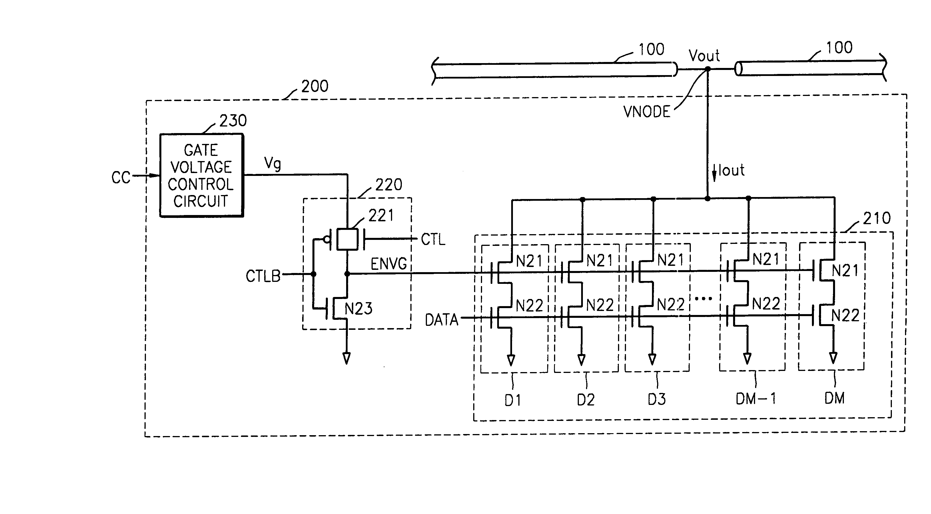
[0031]FIG. 4 is an exemplary circuit diagram of a current mode output driver, according to embodiments of the present invention. Referring to FIG. 4, the current mode output driver 200 is connected to the node VNODE on the transmission line 100. The current mode output driver 200 comprises the driver circuit 210, the bias circuit 220, and the gate voltage control circuit 230.

[0032]The driver circuit 210 includes the plurality of parallel-connected drivers D1 through DM (M is a natural number more than two). The number of drivers included in the driver circuit 210 can be changed. Each of the plurality of drivers D1 through DM include two NMOS transistors N21 and N22. The source of the NMOS transistor N21 is connected to the drain of the NMOS transistor N22. The drain of the NMOS transistor N21 is connected to the node VNODE. The predetermined enable signal ENVG is input into the gate of the NMOS transistor N21. The source of the NMOS transistor N22 is connected to ground and the data...


PUM


Abstract

A current mode output driver and output current control method of controlling an output current using a gate voltage are provided. The current mode output driver, which outputs data read from a memory core to a transmission line, includes a gate voltage control circuit, a bias circuit, and a driver circuit. The gate voltage control circuit generates a predetermined gate voltage in response to a current control signal. The bias circuit outputs the gate voltage as a first enable signal in an active mode, and outputs a ground voltage as a second enable signal in a standby mode. The driver circuit drives a predetermined output current in response to the first enable signal, outputs the predetermined output voltage to the transmission line according to the data, and stops its operation in response to the second enable signal. The gate voltage control circuit changes the level of the gate voltage according to a value of the current control signal and output the changed result. Therefore, it is possible to easily increase resolution of an output current and reduce the occupied area of the current mode output driver, thereby facilitating a circuit design.

Description

BACKGROUND OF THE INVENTION[0001]1. Field of the Invention[0002]Embodiments of the present invention relate to a current mode output driver of a semiconductor memory device for adjusting an output current using a gate voltage and a method for adjusting an output current using the current mode output driver.[0003]This application claims the priority of Korean Patent Application No. 2003-32556, filed on May 22, 2003, in the Korean Intellectual Property Office, the disclosure of which is incorporated herein in its entirety by reference.[0004]2. Description of the Related Art[0005]FIG. 1 shows a general data input / output interface of a semiconductor memory device, such as a rambus DRAM (hereinafter, referred to as ‘RDRAM’). In FIG. 1, the plurality of memory devices 13 are connected to the chipset 11 through the transmission line 12. One end of the transmission line 12 is single-terminated by the terminating resistor Rterm and the terminating voltage Vterm.[0006]Each of the plurality of...

Claims


Application Information

Patent Timeline
IPC IPC(8): G11C7/00G11C7/10G11C11/4096
CPCG11C7/1057G11C7/1051G11C11/4096
Inventor IN-YOUNG, CHUNG
Owner SAMSUNG ELECTRONICS CO LTD
Why Eureka
Try Eureka