A kind of semiconductor integrated device and its manufacturing method

A technology for integrating devices and semiconductors, which is used in semiconductor/solid-state device manufacturing, semiconductor devices, semiconductor/solid-state device components, etc., and can solve problems such as large space, high turn-on resistance of trench MOSFETs, and poor contact characteristics.

Inactive Publication Date: 2011-12-07
FORCE MOS TECH CO LTD
View PDF5 Cites 1 Cited by
  • Summary
  • Abstract
  • Description
  • Claims
  • Application Information

AI Technical Summary

Problems solved by technology

Because the space occupied by the planar contact structure is too large, and it is easy to cause too high turn-on resistance in the trench MOSFET
[0006] Figure 1A and Figure 1B Another limitation of the shown structure is that the source or body region in the trench MOSFET and the anode in t

Method used


Image

  • A kind of semiconductor integrated device and its manufacturing method
  • A kind of semiconductor integrated device and its manufacturing method
  • A kind of semiconductor integrated device and its manufacturing method

Examples


Example Embodiment

[0088] The invention will be described in detail below with reference to the accompanying drawings, in which preferred embodiments of the invention are shown. The invention can, however, be embodied in different ways and should not be limited to the embodiments described herein. For example, the description here refers more to N-channel trench MOSFETs, but clearly other devices are possible.

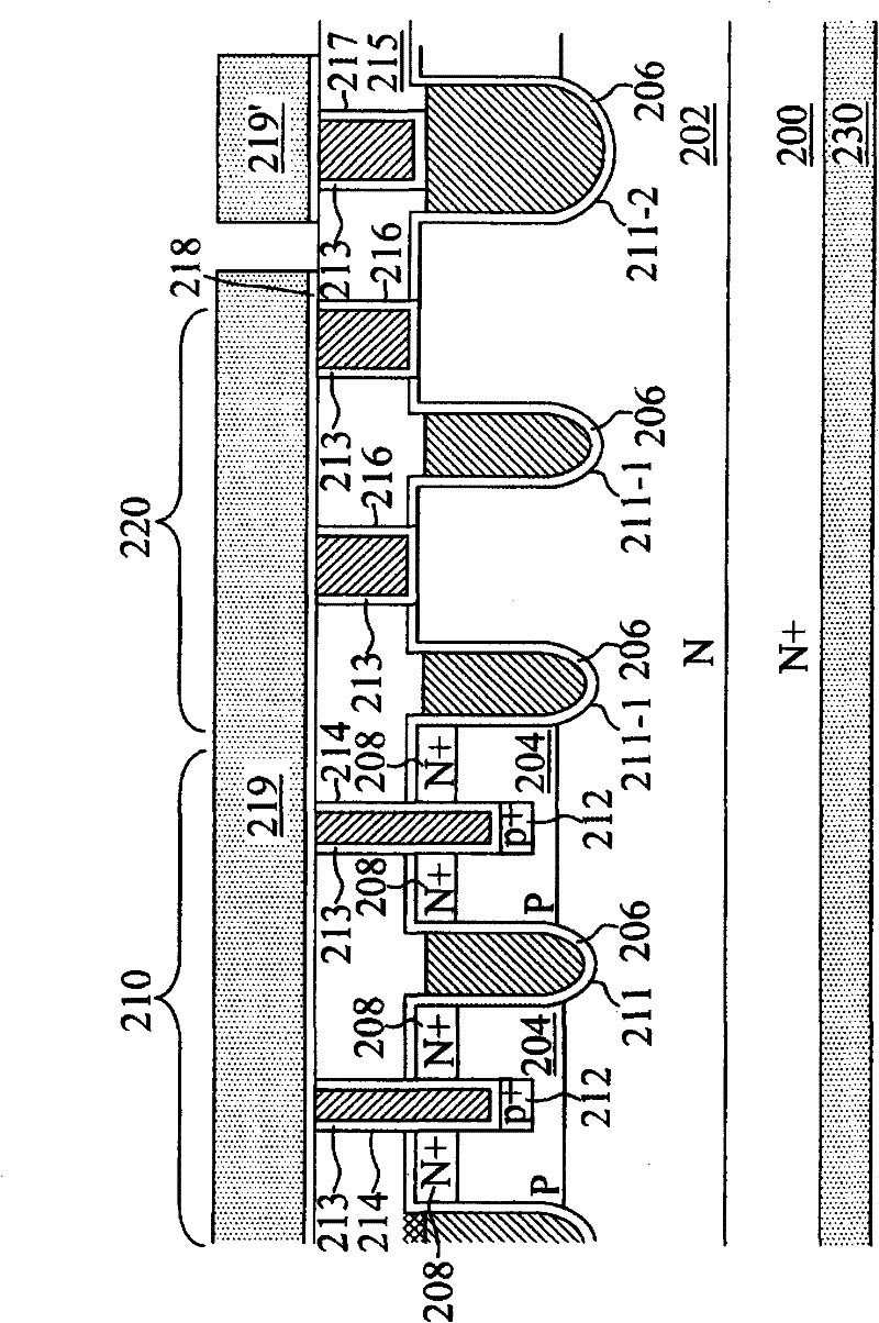
[0089] refer to figure 2 In a preferred embodiment of the present invention shown, the upper surface of the N+ substrate 200 is an N-type epitaxial layer 202 , and the lower surface is a drain metal 230 . In the N-type epitaxial layer 202, there are a plurality of first trench gates 211 located in the trench MOSFET unit 210, a plurality of second trench gates 211-1 located in the trench Schottky rectifier unit 220, and At least one third trench gate 211-2 located in the gate connection region. The inner surfaces of the first trench gate 211, the second trench gate 211-1 and the third...


PUM


Abstract

The invention discloses a semiconductor integrated device comprising a plurality of trench metal oxide semiconductor field effect transistor units and a plurality of trench Schottky ballast units and a manufacturing method thereof. In the trench metal oxide semiconductor field effect transistor unit, the trench type contact area is adopted, which can reduce the turn-on resistance of the device while reducing the size of the device.

Description

technical field [0001] The present invention relates to a unit structure, device structure and process manufacturing of a semiconductor power device, in particular to a semiconductor device comprising a trench metal oxide semiconductor field effect transistor (MOSFET) unit and a trench Schottky rectifier (Schottky Rectifiers) unit Cell structures and fabrication methods for integrated devices. Background technique [0002] In order to achieve higher DC / DC conversion efficiency, the field of semiconductor power device design uses trench Schottky rectifiers (Schottky Rectifiers) in parallel with semiconductor power devices, such as trench metal oxide semiconductor field effect transistors (MOSFETs). method. At this time, the trench Schottky rectifier can be used as a clamp diode (clamp diode) to prevent the PN body diode of the parallel-connected trench MOSFET from turning on. At the same time, since small-sized devices are increasingly becoming the development trend of semi...

Claims


Application Information

Patent Timeline
IPC IPC(8): H01L27/04H01L23/528H01L21/77H01L21/768
CPCH01L2924/0002H01L2924/00
Inventor 谢福渊
Owner FORCE MOS TECH CO LTD
Why Eureka
Try Eureka