Light emitting diode display device and manufacturing method thereof

A technology of light-emitting diodes and display devices, which is applied to identification devices, instruments, electrical components, etc., can solve problems such as increased manufacturing costs, inaccurate bonding accuracy, and poor electrical conduction, and achieves control of deformation, prevention of electrical short circuits, and bonding Effect of backlash prevention

Active Publication Date: 2018-03-06
INNOLUX CORP
View PDF4 Cites 14 Cited by
  • Summary
  • Abstract
  • Description
  • Claims
  • Application Information

AI Technical Summary

Problems solved by technology

However, the conductive particles in the traditional conductive adhesive are randomly distributed, and the conductivity is often insufficient. Therefore, a large number of conductive particles are often needed to improve the conductivity, so there is a problem of increasing manufacturing costs.
In addition, when bonding the electrodes of the light-emitting diode and the pads on the substrate, there are often poor electrical conduction due to too large a bonding gap, excessive compression of conductive particles due to too small a bonding gap, and inaccurate bonding accuracy (excessive displacement) resulting in a large contact area. Insufficient, or P-type pads and N-type pads are connected to cause short circuits, etc.

Method used


Image

  • Light emitting diode display device and manufacturing method thereof
  • Light emitting diode display device and manufacturing method thereof
  • Light emitting diode display device and manufacturing method thereof

Examples


Embodiment Construction

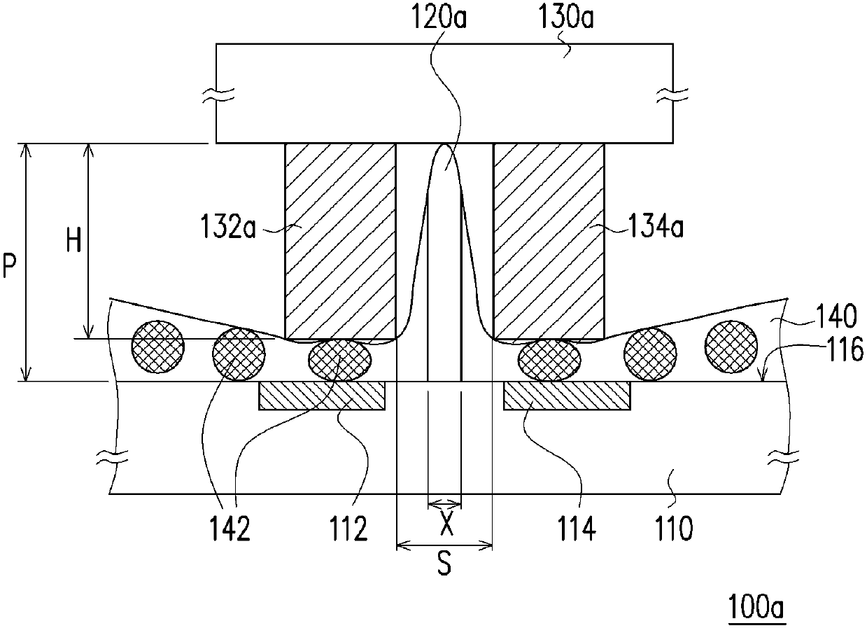
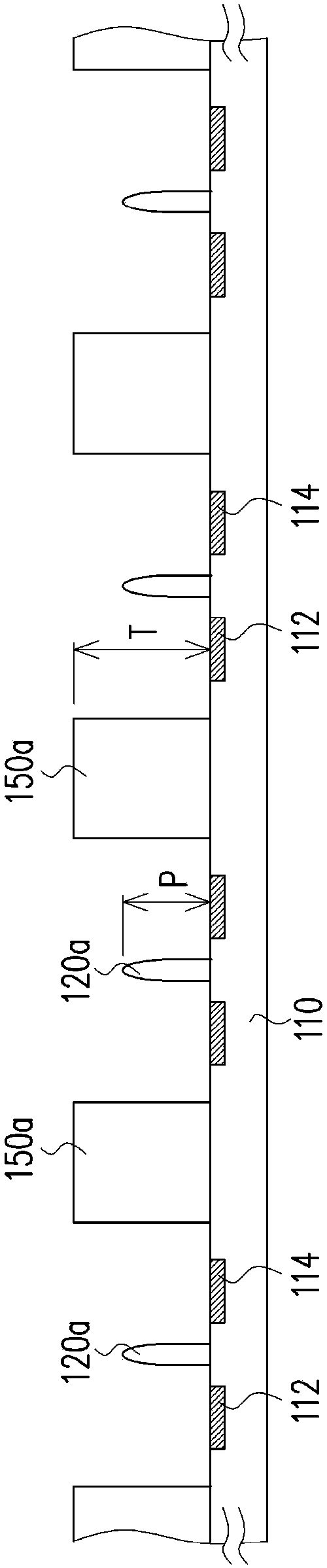
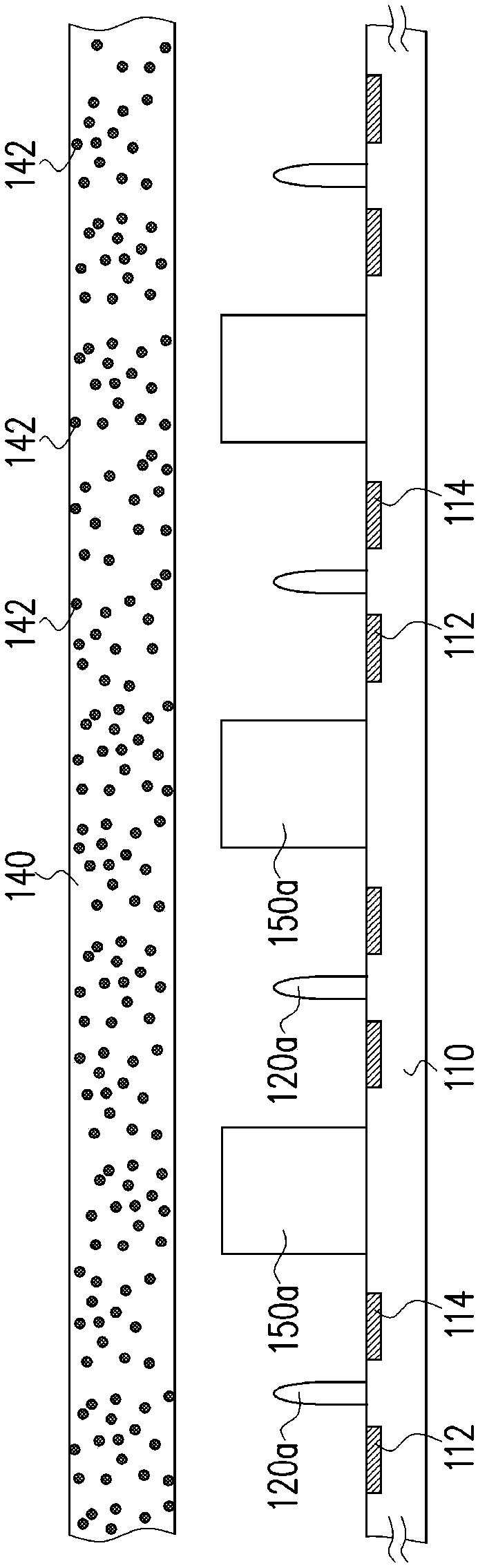
[0038] figure 1 A schematic cross-sectional view of an LED display device according to an embodiment of the present invention is shown. Please refer to figure 1 , in this embodiment, the LED display device 100a includes a substrate 110, at least one first pad 112 ( figure 1 Only one is shown schematically) and at least one second pad 114 ( figure 1 Only one is shown schematically), at least one spacer 120a ( figure 1 only schematically shows one), at least one light emitting diode 130a ( figure 1 Only one is schematically shown in ) and the conductive adhesive layer 140 . The first pad 112 and the second pad 114 are disposed on the substrate 110 . The spacer 120 a is located between the first pad 112 and the second pad 114 , wherein the height of the spacer 120 a is P. The LED 130a is disposed on the substrate 110 and includes a first electrode 132a and a second electrode 134a. The first electrode 132a and the second electrode 134a are located on the same side and have ...


PUM


Abstract

The invention provides a light emitting diode display device and a manufacturing method thereof. The light emitting diode display device includes a substrate, at least a first connecting pad and at least a second connecting pad, at least one spacer, at least one light emitting diode, and a conductive adhesive layer. The first connecting pad and the second connecting pad are disposed on the substrate. The spacer is located between the first connecting pad and the second connecting pad, wherein the height of the spacer is P. The light emitting diode is disposed on the substrate and includes a first electrode and a second electrode. The first electrode and the second electrode are on the same side and heights are H. The conductive adhesive layer is disposed on the substrate and is located between the substrate and the light emitting diode. The conductive adhesive layer includes a plurality of conductive particles, wherein the first electrode and the second electrode of the light emittingdiode are respectively electrically connected with the first connecting pad and the second connecting pad of the substrate through the plurality of conductive particles, and H+3.5>=P>=H+0.48.

Description

technical field [0001] The invention relates to a semiconductor display device and a manufacturing method thereof, in particular to a light emitting diode display device and a manufacturing method thereof. Background technique [0002] With the vigorous development of portable display products, display products have more and more requirements for functions, specifications and costs. Energy-saving and environmentally friendly display technologies are the focus of the development of the next generation of new displays. The light-emitting diodes used in the light-emitting diode array display (LED onarray) are inorganic light-emitting diodes, which have the advantages of long life and low current operation compared to organic light-emitting diodes (AMOLED). [0003] In the processing of the LED array display, the LEDs are bonded on the glass substrate with P-type pads and N-type pads with conductive glue, so that the electrodes of the LEDs are well bonded and electrically connec...

Claims


Application Information

Patent Timeline
Patent Type & Authority Applications(China)
IPC IPC(8): H01L33/48H01L33/62H01L25/075G09F9/33
CPCG09F9/33H01L25/0753H01L33/486H01L33/62H01L2933/0033H01L2933/0066
Inventor 朱伟正姜明甫张顾中
Owner INNOLUX CORP
Why Eureka
Try Eureka