Exposure method, photoetching method and semiconductor manufacturing method

An exposure method and exposure energy technology, applied in the semiconductor field, can solve problems such as differences in key dimensions, different photoresist thicknesses, and too thin film layers, so as to improve production quality, ensure accuracy and uniformity, and improve yield. Effect

Active Publication Date: 2018-03-09
SEMICON MFG INT (SHANGHAI) CORP +1
View PDF4 Cites 0 Cited by
  • Summary
  • Abstract
  • Description
  • Claims
  • Application Information

AI Technical Summary

Problems solved by technology

Severe step height will lead to different thickness of photoresist, and different thickness will lead to difference in critical dimension (CD) size
[0003] In some processes, due to the strict control of the thickness of the film layer, it cannot be too thick, but the controllability of its thickness is not high, which often leads to the film layer being too thin
However, in the area that needs to be etched, it is impossible to fill the film layer, that is to say, there is a difference in the height of the film layer, which affects the CD of the rear layer.

Method used


Image

  • Exposure method, photoetching method and semiconductor manufacturing method
  • Exposure method, photoetching method and semiconductor manufacturing method
  • Exposure method, photoetching method and semiconductor manufacturing method

Examples


Embodiment Construction

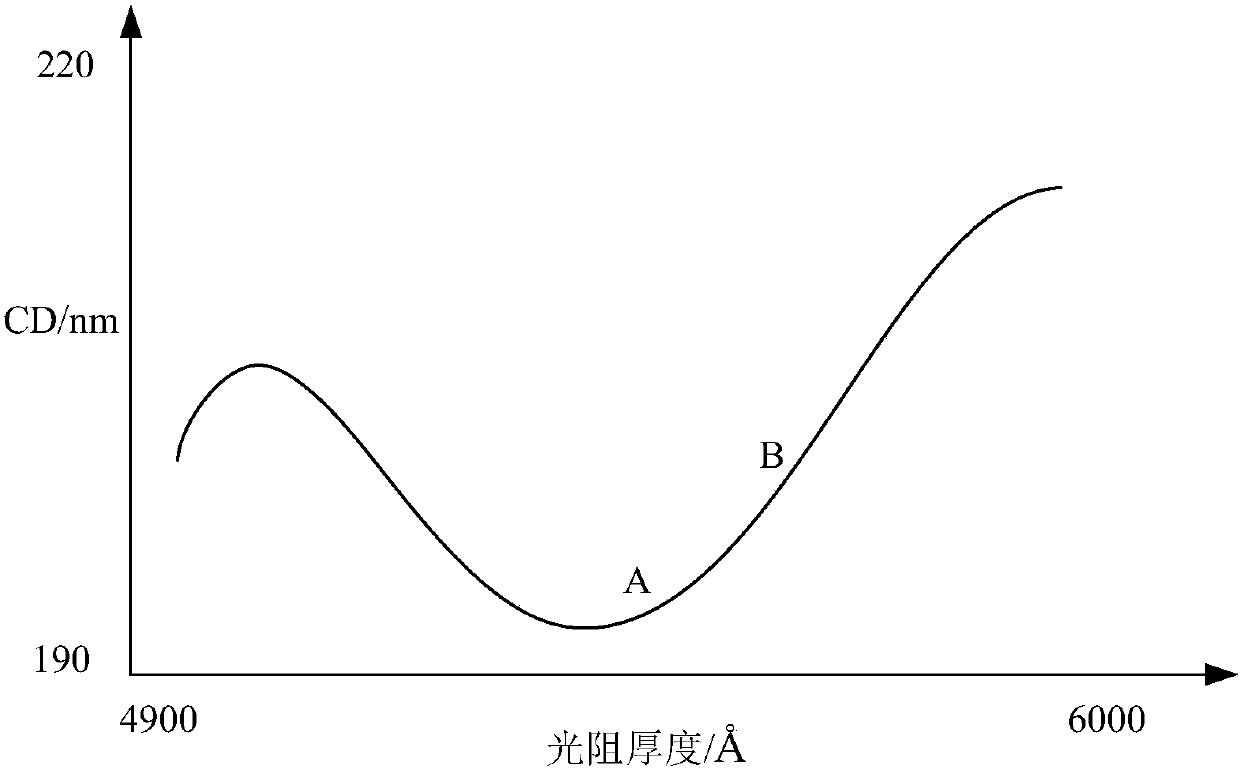
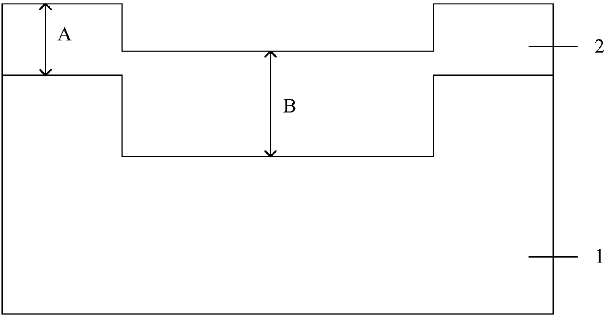
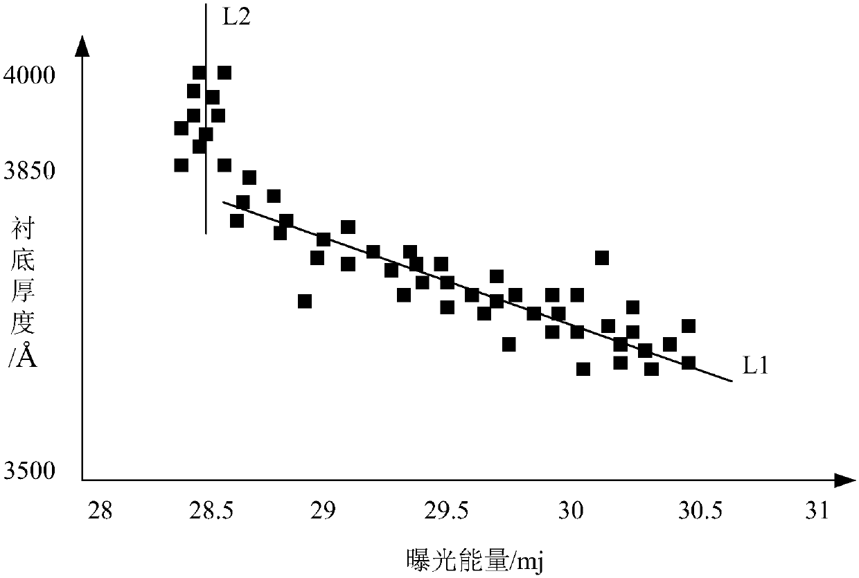
[0031] The exposure method, photolithography method and semiconductor manufacturing method of the present invention will be described in more detail below in conjunction with the schematic diagrams, wherein a preferred embodiment of the present invention is represented, it should be understood that those skilled in the art can modify the present invention described here, and still The advantageous effects of the present invention are realized. Therefore, the following description should be understood as the broad knowledge of those skilled in the art, but not as a limitation of the present invention.

[0032] In the following paragraphs the invention is described more specifically by way of example with reference to the accompanying drawings. Advantages and features of the present invention will be apparent from the following description and claims. It should be noted that all the drawings are in a very simplified form and use imprecise scales, and are only used to facilitate...


PUM


Abstract

The invention discloses an exposure method, a photoetching method and a semiconductor manufacturing method. The exposure method comprises the following steps: acquiring a thickness of a membrane layerto be exposed; judging whether the thickness of the membrane layer reaches a first thickness, and if yes, setting exposure energy according to the thickness of the membrane layer; and if not, acquiring a plane difference of the membrane layer; and setting the exposure energy according to the thickness and plane difference of the membrane layer. Therefore, when in height difference, the conditionthat the exposure energy is uncontrollable is avoided, so that the accuracy and uniformity of CD can be ensured, the production quality can be improved, and the yield can be increased.

Description

technical field [0001] The invention relates to the technical field of semiconductors, in particular to an exposure method, a photolithography method and a semiconductor manufacturing method. Background technique [0002] In the photolithography process, the requirements for flatness are very high. Severe step height will lead to different thickness of photoresist, and different thickness will lead to difference in critical dimension (CD). [0003] In some processes, due to the strict control of the thickness of the film layer, it cannot be too thick, but the controllability of the thickness is not high, which often leads to the film layer being too thin. However, in the area that needs to be etched, it is impossible to fill up the film layer, that is to say, there will be a difference in height of the film layer, which will affect the CD of the subsequent layer. [0004] Therefore, how to improve this situation is imperative. Contents of the invention [0005] The obje...

Claims


Application Information

Patent Timeline
Patent Type & Authority Applications(China)
IPC IPC(8): G03F7/20
CPCG03F7/70558G03F7/70633
Inventor 王清蕴张海
Owner SEMICON MFG INT (SHANGHAI) CORP
Why Eureka
Try Eureka