Display panel, manufacturing method of display panel and display device

A display panel and manufacturing method technology, applied in semiconductor/solid-state device manufacturing, organic semiconductor devices, semiconductor devices, etc., can solve the problems of poor packaging effect of packaging structure, improve packaging effect, and solve the effect of poor packaging effect

Active Publication Date: 2018-03-09
BOE TECH GRP CO LTD +1
View PDF6 Cites 28 Cited by
  • Summary
  • Abstract
  • Description
  • Claims
  • Application Information

AI Technical Summary

Problems solved by technology

[0005] The present invention provides a display panel, a manufacturing method thereof, and a display device, which can solve the problem of poor encapsulation effect of the encapsulation structure

Method used


Image

  • Display panel, manufacturing method of display panel and display device
  • Display panel, manufacturing method of display panel and display device
  • Display panel, manufacturing method of display panel and display device

Examples


Embodiment Construction

[0062] In order to make the purpose, technical solutions and advantages of the present invention clearer, the present invention will be further described in detail below in conjunction with the accompanying drawings. Obviously, the described embodiments are only some of the embodiments of the present invention, rather than all of them. Based on the embodiments of the present invention, all other embodiments obtained by persons of ordinary skill in the art without making creative efforts belong to the protection scope of the present invention.

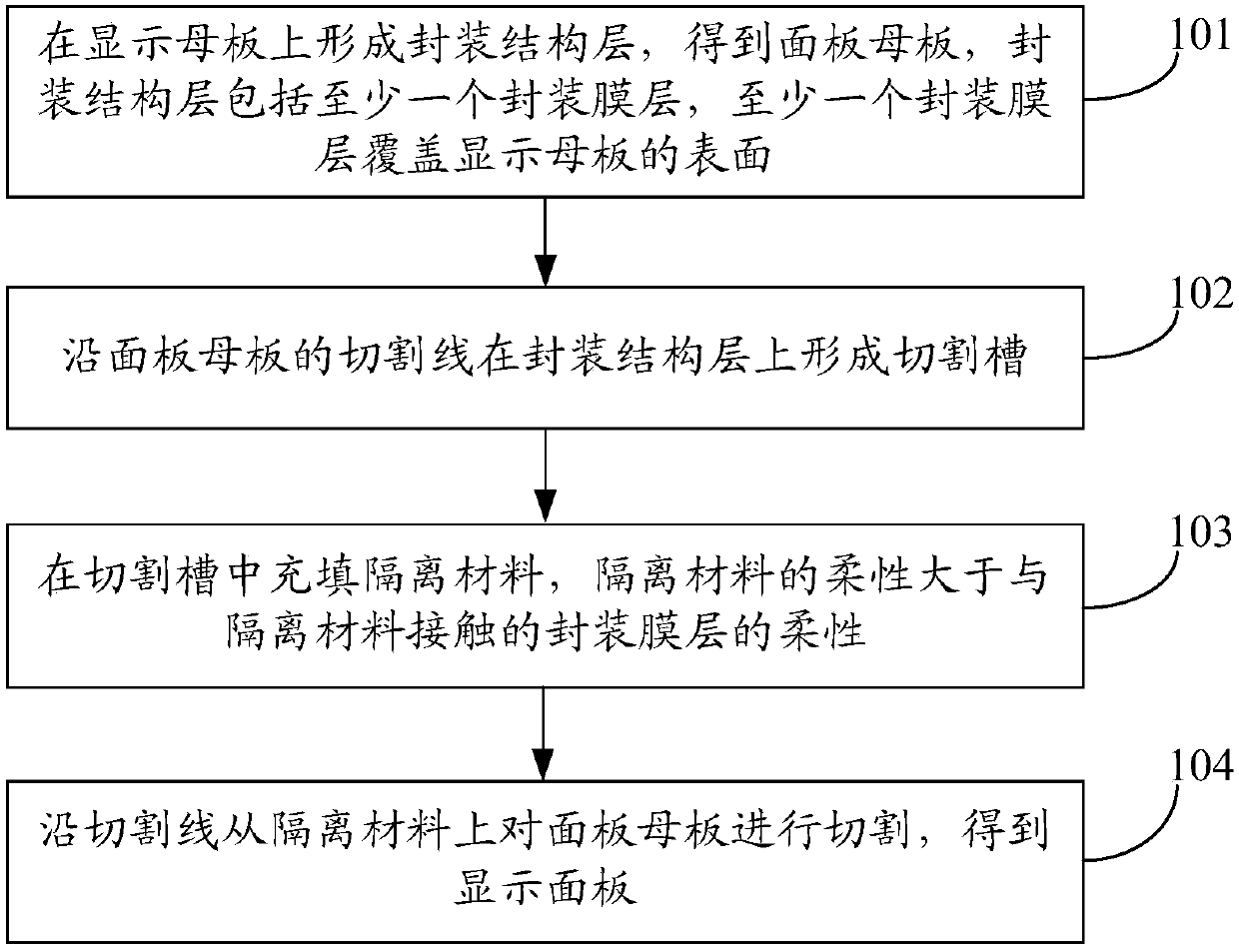
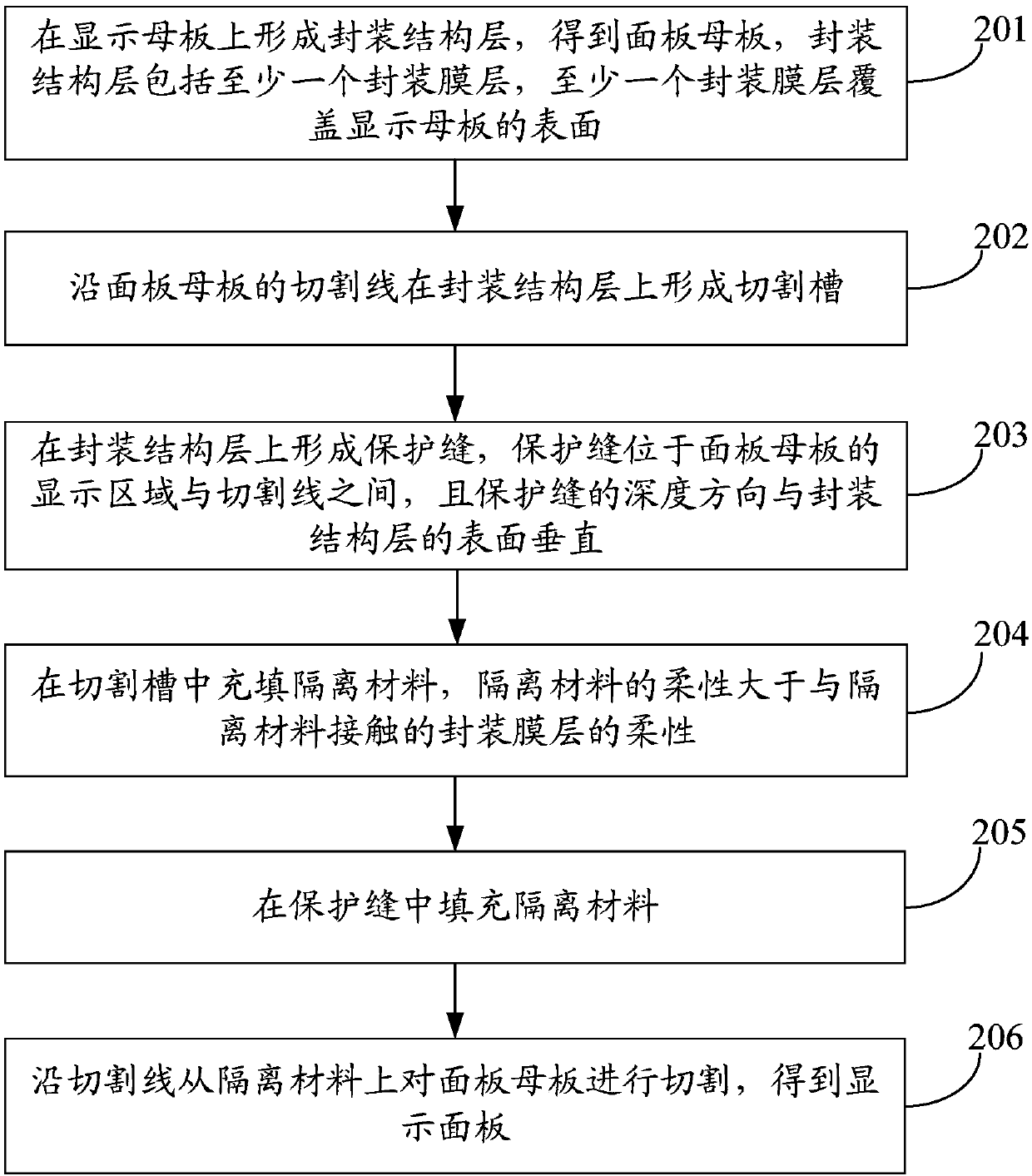
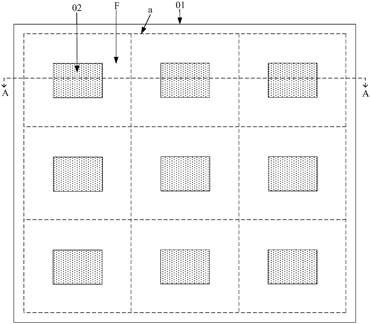
[0063] An OLED display panel is a display panel formed by cutting an OLED panel motherboard. The OLED panel motherboard includes a display motherboard and an encapsulation structure layer arranged on the display motherboard. The display motherboard has multiple display areas, and each display area OLED devices are arranged in the center, and the encapsulation structure layer includes a plurality of encapsulation structures corresponding ...


PUM


Abstract

The invention discloses a display panel, a manufacturing method of the display panel and a display device, and belongs to the technical field of display. The method comprises the steps that a packaging structure layer is formed on a display mother board to obtain a panel mother board, wherein the packaging structure layer comprises at least one packaging film layer, and the at least one packagingfilm layer covers the surface of the display mother board; a cutting groove is formed in the packaging structure layer along a cutting line of the panel mother board; the cutting groove is filled withan isolation material, wherein the flexibility of the isolation material is larger than that of the packaging film layer in contact with the isolation material; the panel mother board is cut from theisolation material along the cutting line to obtain the display panel. The problem that the packaging effect of a packaging structure is poor is solved, and the packaging effect of the packaging structure is improved. The method is used for manufacturing the display panel.

Description

technical field [0001] The present invention relates to the field of display technology, in particular to a display panel, a manufacturing method thereof, and a display device. Background technique [0002] The organic light-emitting diode (English: Organic Light-Emitting Diode; abbreviation: OLED) display panel has the advantages of high brightness, high contrast, full viewing angle and flexible display, and is widely used in the display industry. The OLED display panel includes a display substrate and an encapsulation structure arranged on the display substrate. The encapsulation structure is used for encapsulating the OLED device on the display substrate to prevent components in the air from corroding the OLED device. [0003] An OLED display panel is a display panel formed by cutting an OLED panel motherboard. The OLED panel motherboard includes a display motherboard and an encapsulation structure layer arranged on the display motherboard. The display motherboard has mul...

Claims


Application Information

Patent Timeline
Patent Type & Authority Applications(China)
IPC IPC(8): H01L51/56H01L51/52H01L27/32
CPCH10K59/12H10K50/84H10K71/00H10K50/8445H10K71/851H10K50/844
Inventor 马国强王杨孙阔
Owner BOE TECH GRP CO LTD
Why Eureka
Try Eureka