Efficient organic light-emitting diode and manufacturing method thereof

A light-emitting diode, high-efficiency technology, applied in the direction of organic light-emitting device, organic light-emitting device structure, semiconductor/solid-state device manufacturing, etc., can solve the problems of reducing the optical coupling output efficiency of the device, light loss, etc. properties, the effect of improving transmittance

Inactive Publication Date: 2015-01-07
NANJING UNIV OF POSTS & TELECOMM
View PDF8 Cites 12 Cited by
  • Summary
  • Abstract
  • Description
  • Claims
  • Application Information

AI Technical Summary

Problems solved by technology

However, organic light-emitting diodes are composed of multi-layer structures. Due to the difference in refractive index between layers and between the device and the air, only a small part of the generated light can exit the device, while most of the rest of the light is confined in the device. Inside and cannot enter the air, the trapped light is either confined in the glass substrate and device in waveguide mode, or radiated from the edge of the substrate, typically up to 80% of the generated light is lost in this way, greatly reducing the optical coupling of the device output efficiency

Method used


Image

  • Efficient organic light-emitting diode and manufacturing method thereof
  • Efficient organic light-emitting diode and manufacturing method thereof
  • Efficient organic light-emitting diode and manufacturing method thereof

Examples


Embodiment 1

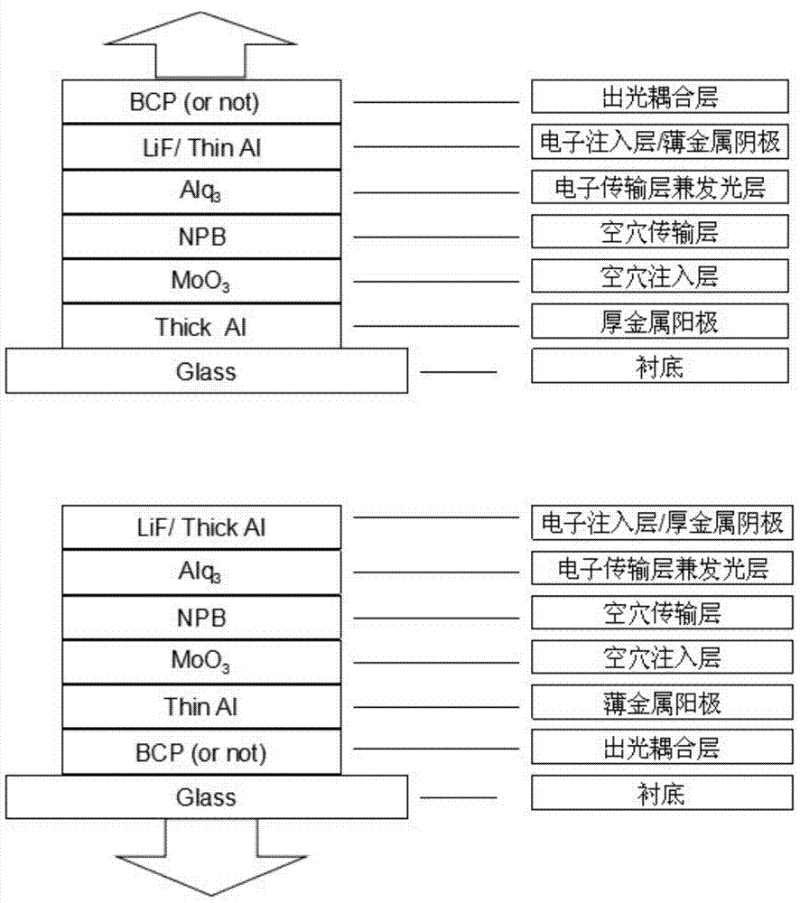
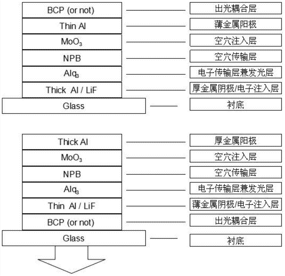
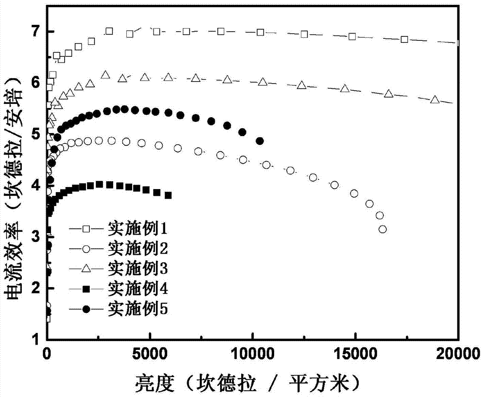
[0055] Clean the glass substrate with better flatness, blow it dry with nitrogen, place the glass substrate in a UV oven and treat it with ultraviolet ozone for 5 minutes, and finally put the glass substrate into a vacuum coating system. The organic material is placed in different evaporation sources, and the temperature of each evaporation source can be controlled individually. When the vacuum degree of the vacuum coating system reaches 3×10 -5 When it is below Pascal, first evaporate aluminum with a width of 4 mm and a length of 26 mm on the glass substrate as a thick metal anode. Then, the hole injection layer MoO was sequentially evaporated on the anode 3 , hole transport layer NPB, light emitting layer and electron transport layer Alq 3 , electron injection layer LiF and thin metal cathode Al, where the two electrodes intersect each other to form the light-emitting area of ​​the device, the effective area of ​​the light-emitting area is 16 square millimeters, thick meta...

Embodiment 2

[0057] Clean the glass substrate with better flatness, blow it dry with nitrogen, place the glass substrate in a UV oven and treat it with ultraviolet ozone for 5 minutes, and finally put the glass substrate into a vacuum coating system. When the vacuum degree of the vacuum coating system reaches 3×10⁻⁵ When it is below Pascal, first evaporate aluminum with a width of 4 mm and a length of 26 mm on the glass substrate as a thick metal anode. Then, the hole injection layer MoO was sequentially evaporated on the anode 3 , hole transport layer NPB, light emitting layer and electron transport layer Alq 3 , electron injection layer LiF and thin metal cathode Al, where the two electrodes intersect each other to form the light-emitting area of ​​the device, the effective area of ​​the light-emitting area is 16 square millimeters, thick metal anode, hole injection layer, hole transport layer, light-emitting layer The thicknesses of electron transport layer, electron injection layer an...

Embodiment 3

[0059] Clean the glass substrate with better flatness, blow it dry with nitrogen, place the glass substrate in a UV oven and treat it with ultraviolet ozone for 5 minutes, and finally put the glass substrate into a vacuum coating system. When the vacuum degree of the vacuum coating system reaches 3×10 -5 When it is below Pascal, first evaporate aluminum with a width of 4 mm and a length of 26 mm on the glass substrate as a thick metal anode. Then, the hole injection layer MoO was sequentially evaporated on the anode 3 , hole transport layer NPB, light emitting layer and electron transport layer Alq3, electron injection layer LiF, thin metal cathode Al and light coupling layer BCP, where the two electrodes cross each other to form the light emitting area of ​​the device, and the effective area of ​​the light emitting area is 16 mm2, the thicknesses of thick metal anode, hole injection layer, hole transport layer, light-emitting layer and electron transport layer, electron inje...


PUM


Abstract

The invention relates to an efficient organic light-emitting diode and a manufacturing method of the efficient organic light-emitting diode. The efficient organic light-emitting diode is of a microcavity structure. The efficient organic light-emitting diode structurally comprises a substrate, a metal anode, a hole injection layer, a hole transmission layer, an electron transfer layer / light-emitting layer and an electron injection layer / metal cathode from bottom to top in sequence. The microcavity structure is formed by bimetallic electrode aluminum, by the adoption of the optical microcavity of the structure, efficient organic light-emitting devices can be manufactured both in a top light-emitting component structure and a bottom light-emitting component structure, and the luminescent spectrum can be narrowed. Or the efficient organic light-emitting diode structurally comprises the substrate, the metal cathode / electron injection layer, the electron transfer layer / light-emitting layer, the hole transmission layer, the hole injection layer and the metal anode from bottom to top in sequence. Due to the fact that the bimetallic electrode structure is adopted by the optical microcavity, the efficient organic light-emitting diode is obtained through the microcavity effect, and the characteristic of higher spectrum color purity is shown at the same time.

Description

technical field [0001] The present invention relates to the field of organic electroluminescent devices (OLEDs). More specifically, the present invention relates to an OLED device including a microcavity structure and a preparation method thereof. Background technique [0002] Organic electroluminescent device (OLED) is an impressive solid-state flat-panel display technology developed in recent years. Compared with other display technologies, OLED has low DC voltage drive, low power consumption, self-luminescence, simple structure, super Due to the advantages of thinness, fast response, wide viewing angle, and flexibility, it has become one of the most promising technologies in the field of optoelectronic devices and flat panel displays. [0003] Organic light-emitting diodes generally include an anode, a cathode, and an organic electroluminescent unit sandwiched between the two electrodes. The organic electroluminescent unit includes at least a hole transport layer, a ligh...

Claims


Application Information

Patent Timeline
Patent Type & Authority Applications(China)
IPC IPC(8): H01L51/50H01L51/52H01L51/56
CPCH10K50/00H10K50/805H10K50/85H10K2102/302H10K71/00
Inventor 张宏梅吴远武
Owner NANJING UNIV OF POSTS & TELECOMM
Why Eureka
Try Eureka