Organic light emitting diode with double-layer electron transport layer and preparation method thereof

A technology of electron transport layer and light-emitting diode, which is applied in the direction of organic semiconductor devices, circuits, electrical components, etc., can solve the problem that electron injection and transport capabilities are inferior to holes, and achieve large-area production, reduce costs, and improve utilization. Effect

Inactive Publication Date: 2014-09-24
UNIV OF SCI & TECH BEIJING
View PDF2 Cites 30 Cited by
  • Summary
  • Abstract
  • Description
  • Claims
  • Application Information

AI Technical Summary

Problems solved by technology

[0006] The purpose of the present invention is to solve the problem that electron injection and trans

Method used


Image

  • Organic light emitting diode with double-layer electron transport layer and preparation method thereof

Examples


Example Embodiment

[0071] Example 1

[0072] Implementation steps:

[0073] 1) First, prepare zinc oxide nanoparticles by sol-gel method according to the method, and redisperse white zinc oxide powder with 1% oleylamine-containing octane solution to obtain zinc oxide nanoparticles with a final concentration of about 3 mg / ml Particle dispersion. This zinc oxide nanoparticle dispersion has the following characteristics: the nanoparticle has stable properties, small particle size and good uniformity, with a particle size of about 5-6 nm; the dispersant is octane hydrocarbon, which does not cause damage to the lithium acetylacetonate ultra-thin film; After dispersion, the concentration of the solution is controllable; the formed film has good transparency to visible light.

[0074] 2) Prepare the alcohol solution of acetylacetonate metal salt: Dissolve lithium acetylacetonate (Li(acac)) in anhydrous methanol to prepare a solution with a concentration of 1 mg / ml.
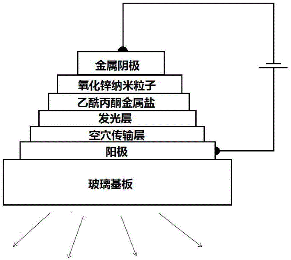
[0075] The organic light-emitting diode w...

Example Embodiment

[0088] Example 2

[0089] 1) First, prepare zinc oxide nanoparticles by sol-gel method according to the method, and redisperse the white zinc oxide powder with a hexane solution containing 1% oleylamine to obtain zinc oxide nanoparticles with a final concentration of about 3 mg / ml Particle dispersion.

[0090] 2) Prepare the alcohol solution of acetylacetonate metal salt: add strontium acetylacetonate (Sr(acac) 2 ) Dissolved in isopropanol to prepare a solution with a concentration of 1 mg / ml.

[0091] The device was prepared according to the method of Example 1, except that the rotation speed of the spin-coated strontium acetylacetonate solution was 5000 rpm. Hexane is used as the final dispersant of zinc oxide nanoparticles.

Example Embodiment

[0092] Example 3

[0093] The device is prepared according to the method of Example 1, except that the luminescent material is a white luminescent material which is a mixture of blue and orange-red phosphorescent materials. As for lighting applications, complementary color scheme devices have a simple structure and high efficiency. Phosphorescent materials are usually used to obtain high efficiency and can control the chromaticity of white light to a certain extent. Among them, the blue phosphorescent material is FIrpic, and the orange-red phosphorescent material is selected (acetylacetonate bis(2-phenylbenzothiazole-C2,N) iridium(III)) (Ir(BT) 2 (acac)), the host material is PVK, the carrier transport material is OXD-7, and the ratio (weight ratio) of each compound in the light-emitting layer is PVK:FIrpic:OXD-7:Ir(BT) 2 (acac) = 10:1:4:0.04. In white light devices, when octane is used as the dispersant of zinc oxide nanoparticles, the device with optimized electron transport la...


PUM

PropertyMeasurementUnit
Thicknessaaaaaaaaaa
Particle sizeaaaaaaaaaa
Film thicknessaaaaaaaaaa

Abstract

The invention relates to an organic light emitting diode with a double-layer electron transport layer and a preparation method thereof. The preparation method is characterized in that the double-layer electron transport layer is prepared by a solution method, namely, an ultra-thin acetylacetonate metal salt film is deposited on a light emitting layer of the device by the solution method first, and then a zinc oxide nano particle film is deposited on the ultra-thin acetylacetonate metal salt film by the solution method, thus realizing preparation of the double-layer electron transport layer through a full solution method. By adopting the method to prepare the electron transport layer of the organic light emitting diode, injection and transport of electrons in the device can be improved, charge transfer between the light emitting layer and the zinc oxide layer can be effectively inhibited, the device is enabled to get light emitting efficiency a hundred times higher than that of a conventional device, and the device has lower driving voltage and higher brightness. The method of the invention is widely used in the field of organic light emitting devices.

Description

technical field [0001] The invention belongs to the field of organic semiconductor devices, and relates to a double-layer structure electron transport layer in an organic light-emitting diode and its solution method preparation. Background technique [0002] Organic light-emitting diodes are self-luminous, and have the advantages of high color quality, fast response, wide viewing angle, ultra-thin, green and environmental protection, and can realize large-area flexible light emission. With the gradual improvement of the solution preparation method, its low-cost potential has been gradually discovered, showing that it has great application potential in the fields of next-generation information display and solid-state lighting. However, the performance of organic electroluminescent devices is not perfect at this stage, and there are still great limitations in production technology and cost. Compared with the vacuum evaporation method, the solution method can improve the utili...

Claims


Application Information

Patent Timeline
IPC IPC(8): H01L51/54H01L51/52H01L51/56
CPCH10K50/166H10K2102/00H10K71/00
Inventor 李立东徐新军贾曼平田原王金山
Owner UNIV OF SCI & TECH BEIJING
Why Eureka
Try Eureka