Buffer layers for metal oxide semiconductors for TFT

Inactive Publication Date: 2014-09-18
APPLIED MATERIALS INC
View PDF7 Cites 1 Cited by
  • Summary
  • Abstract
  • Description
  • Claims
  • Application Information

AI Technical Summary

Benefits of technology

The present invention is related to a thin film semiconductor device which includes a buffer layer between the semiconductor layer and other layers. The buffer layer has high work function and low electron affinity to prevent charge transfer between the semiconductor layer and the gate dielectric layer. This results in maintaining the charge formed in the semiconductor layer and prevents an increase in threshold voltage for the thin film semiconductor.

Problems solved by technology

In current MO-TFTs, the interface between layers, such as the interface between the gate dielectric layer and the metal oxide semiconductor layer, can be problematic for the overall function of the device.
In indium gallium zinc oxide (IGZO), zinc oxide (ZnO) and zinc oxynitride (ZnON) TFT devices, problems can include mobility problems and turn on voltages.

Method used


Image

  • Buffer layers for metal oxide semiconductors for TFT
  • Buffer layers for metal oxide semiconductors for TFT
  • Buffer layers for metal oxide semiconductors for TFT

Examples


Embodiment Construction

[0018]The present embodiments generally relate to a thin film semiconductor device having multiple semiconductor layers. A buffer layer having a high work function and a low electron affinity can be deposited between the semiconductor layer and other layers. By inserting the buffer layer, mobility problems can be avoided and the threshold voltage of the gate can be maintained at a lower level. While description will be made with reference to a TFT, it is to be understood that the invention has broader utility, such as with any thin film semiconductor device.

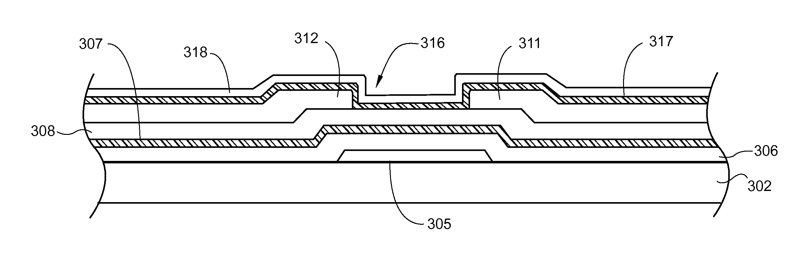
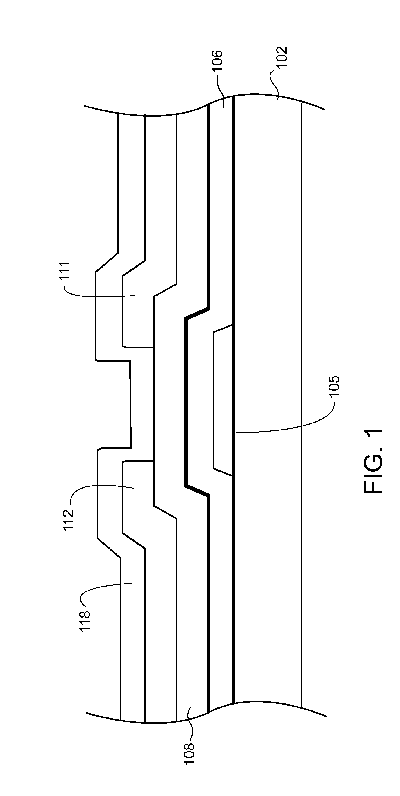
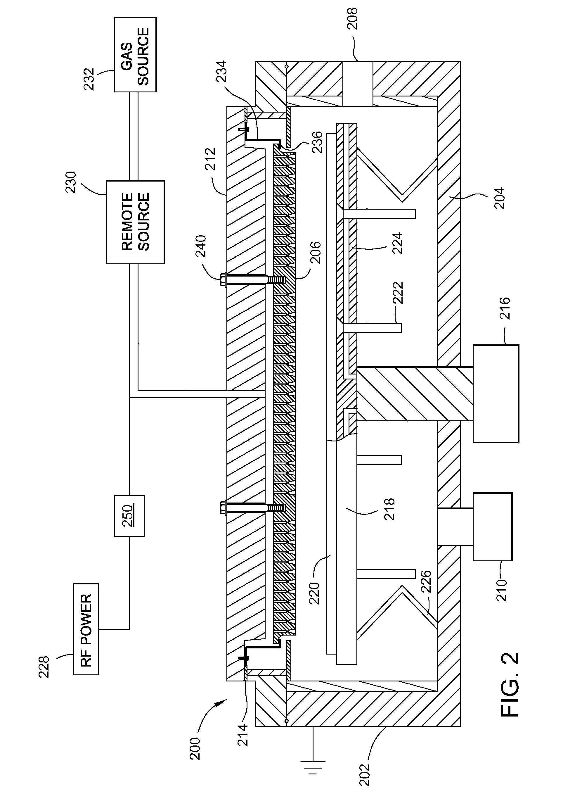
[0019]FIG. 1 is a depiction of a generic MO-TFT. In this depiction, a substrate 102 has a stack deposited on the surface by various techniques such as PVD, CVD, PE-CVD or other techniques. The MO-TFT stack can be deposited on the substrate and can include a gate electrode 105, gate dielectric layer 106, a semiconductor layer 108, a source electrode 111, a drain electrode 112 and a passivation layer 118.

[0020]The interface between...


PUM


Abstract

The present invention generally relates to a thin film semiconductor device having a buffer layer formed between the semiconductor layer and one or more layers. In one embodiment, a thin film semiconductor device includes a semiconductor layer having a first work function and a first electron affinity level, a buffer layer having a second work function greater than the first work function and a second electron affinity level that is less than the first electron affinity level; and a gate dielectric layer having a third work function less than the second work function and a third electron affinity level that is greater than the second electron affinity level.

Description

CROSS-REFERENCE TO RELATED APPLICATIONS[0001]This application claims benefit of U.S. Provisional Patent Application Ser. No. 61 / 791,588 (APPM / 20701USL), filed Mar. 15, 2013, which is herein incorporated by reference.BACKGROUND OF THE INVENTION[0002]1. Field of the Invention[0003]Embodiments disclosed herein generally relate to buffer layers for thin film semiconductors. More specifically, embodiments disclosed herein generally relate to high work function and low electron affinity layers.[0004]2. Description of the Related Art[0005]Current interest in thin film transistors (TFTs) is particularly high because these devices may be used in liquid crystal active matrix displays (LCDs) of the kind often employed for computer and television flat panels. The LCDs may also contain light emitting diodes (LEDs), such as organic light emitting diodes (OLEDs) for back lighting. The LEDs and OLEDs require TFTs for addressing the activity of the displays. One of the applications for the semicondu...

Claims


Application Information

Patent Timeline
IPC IPC(8): H01L29/786
CPCH01L29/7869H01L29/4908
Inventor LESCHKIES, KURTISVERHAVERBEKE, STEVENVISSER, ROBERTWHITE, JOHN M.YE, YANYIM, DONG-KIL
Owner APPLIED MATERIALS INC
Why Eureka
Try Eureka