Metal oxynitride gate

Inactive Publication Date: 2007-12-13
TAIWAN SEMICON MFG CO LTD
View PDF10 Cites 14 Cited by
  • Summary
  • Abstract
  • Description
  • Claims
  • Application Information

AI Technical Summary

Benefits of technology

[0012]In accordance with another aspect of the present invention, the composition of the metal oxynitride can be changed by adjusting the partial pressures of nitrogen, oxygen and carbon-containing gas. The work function of the gate electrode is thus changed, and a band-edge work function can be achieved.
[0013]A metal oxynitride gate electrode will have a high work function. The work function can be adjusted to band-edge by selecting a proper composition. The equivalent oxide thickness of the preferred embodiments of the present invention is significantly lower than that of the transistor using a metal oxide gate. Therefore, high performance can be achieved on PMOS transistors using a metal oxynitride gate electrode.

Problems solved by technology

The depletion effect increases the effective gate dielectric thickness, making it more difficult for an inversion layer to be created at the surface of the semiconductor.
The use of thinner gate dielectrics tends to make the carrier depletion effect even worse.
With thinner gate dielectrics, the depletion layer in the polysilicon gate becomes more significant in dimension when compared to the thickness of the thin gate dielectric, and thus device performance degradation is worsened.
As a result, the carrier depletion effect in the gate electrode limits device scalability by imposing a lower bound on how much the effective gate dielectric thickness can be reduced.
However, most of these materials still have difficulty achieving an effective work function higher than 5 eV.
Although metal nitride gates having high work functions have been reported, it is difficult to adjust the work function of metal nitrides to the band-edge and further improve PMOS transistor performance.

Method used


Image

  • Metal oxynitride gate
  • Metal oxynitride gate
  • Metal oxynitride gate

Examples


Embodiment Construction

[0018]The making and using of the presently preferred embodiments are discussed in detail below. It should be appreciated, however, that the present invention provides many applicable inventive concepts that can be embodied in a wide variety of specific contexts. The specific embodiments discussed are merely illustrative of specific ways to make and use the invention, and do not limit the scope of the invention.

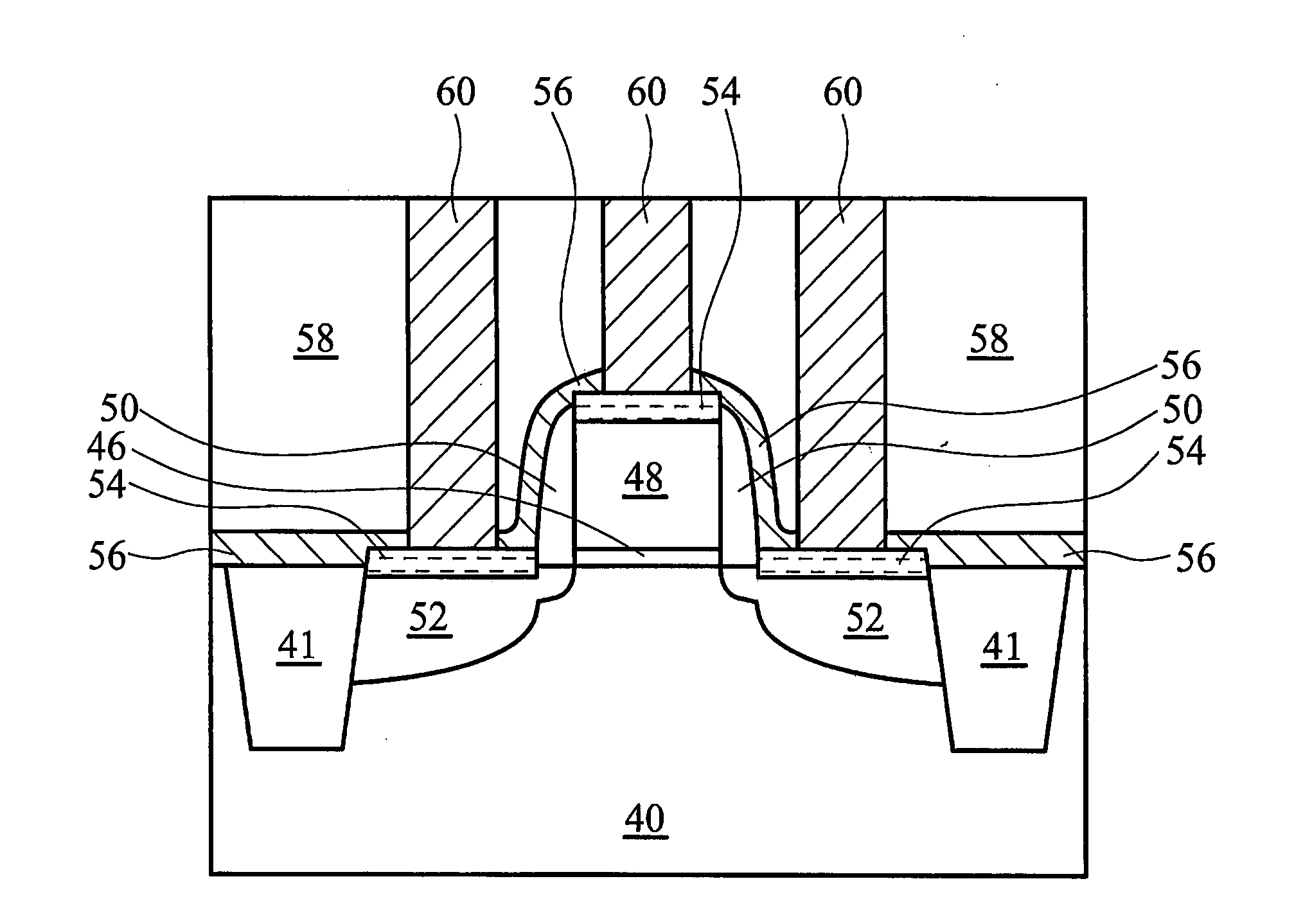
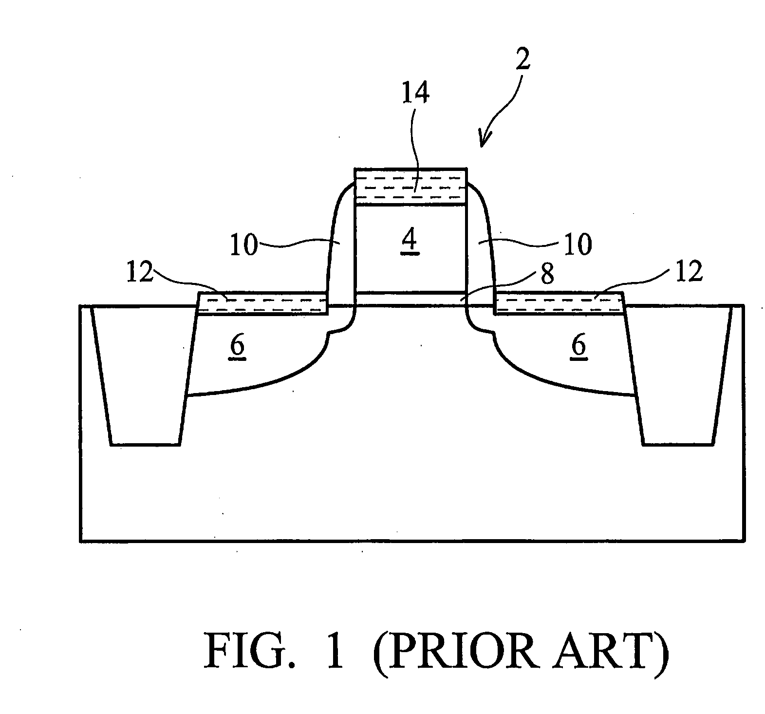
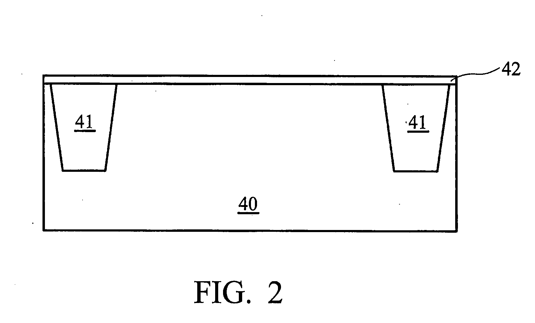
[0019]FIGS. 2 through 6 illustrate cross-sectional views of a preferred embodiment of the present invention, wherein a PMOS transistor is formed. Referring to FIG. 2, a gate dielectric layer 42 is formed on a substrate 40, which comprises shallow trench isolation regions 41. The substrate 40 may comprise commonly used substrate materials such as silicon, strained silicon on SiGe, silicon on insulator (SOI), silicon germanium on insulator (SGOI), and the like. The substrate 40 may also have a composite structure such as a silicon-on-oxide structure. The substrate 40 is prefera...


PUM


Abstract

A metal-oxide-semiconductor (MOS) transistor having a gate electrode comprising a metal oxynitride and a method of forming the same are provided. The metal oxynitride preferably comprises molybdenum oxynitride and / or iridium oxynitride. The gate electrode may further comprise carbon and / or silicon. The gate electrode is preferably formed in a chamber containing nitrogen, oxygen and a carbon-containing gas. The gate electrode of the MOS transistor has a high work function and a low equivalent oxide thickness.

Description

[0001]This application claims the benefit of Provisional Patent Application Ser. No. 60 / 811,820, filed Jun. 8, 2006, and entitled “Metal Oxynitride Gate,” which application is incorporated herein by reference.TECHNICAL FIELD[0002]This invention relates generally to semiconductor devices, and more particularly to metal-oxide-semiconductor (MOS) devices.BACKGROUND[0003]Metal-oxide-semiconductor (MOS) transistors are basic building elements in integrated circuits. An example of a conventional MOS transistor structure is shown in FIG. 1. A MOS transistor 2 typically includes a gate dielectric 8, a gate electrode 4, source / drain regions 6, and gate spacers 10. The top surfaces of source / drain regions 6 and gate electrode 4 are typically silicided, forming silicides 12 and 14 respectively.[0004]In a conventional MOS transistor as shown in FIG. 1, the gate electrode 4 typically comprises polysilicon doped with p-type or n-type impurities, using doping operations such as ion implantation or...

Claims


Application Information

Patent Timeline
IPC IPC(8): H01L29/76H01L21/336
CPCH01L21/28088H01L29/665H01L29/517H01L29/4966
Inventor CHANG, WENGHU, BOQ-KANGSCHAEFFER, JAMIEGILMER, DAVID C.TOBIN, PHIL
Owner TAIWAN SEMICON MFG CO LTD
Why Eureka
Try Eureka