

Methods to form dual metal gates by incorporating metals and their conductive oxides
- Summary
- Abstract
- Description
- Claims
- Application Information
AI Technical Summary
Benefits of technology
Problems solved by technology
Method used
Image

Examples
first embodiment
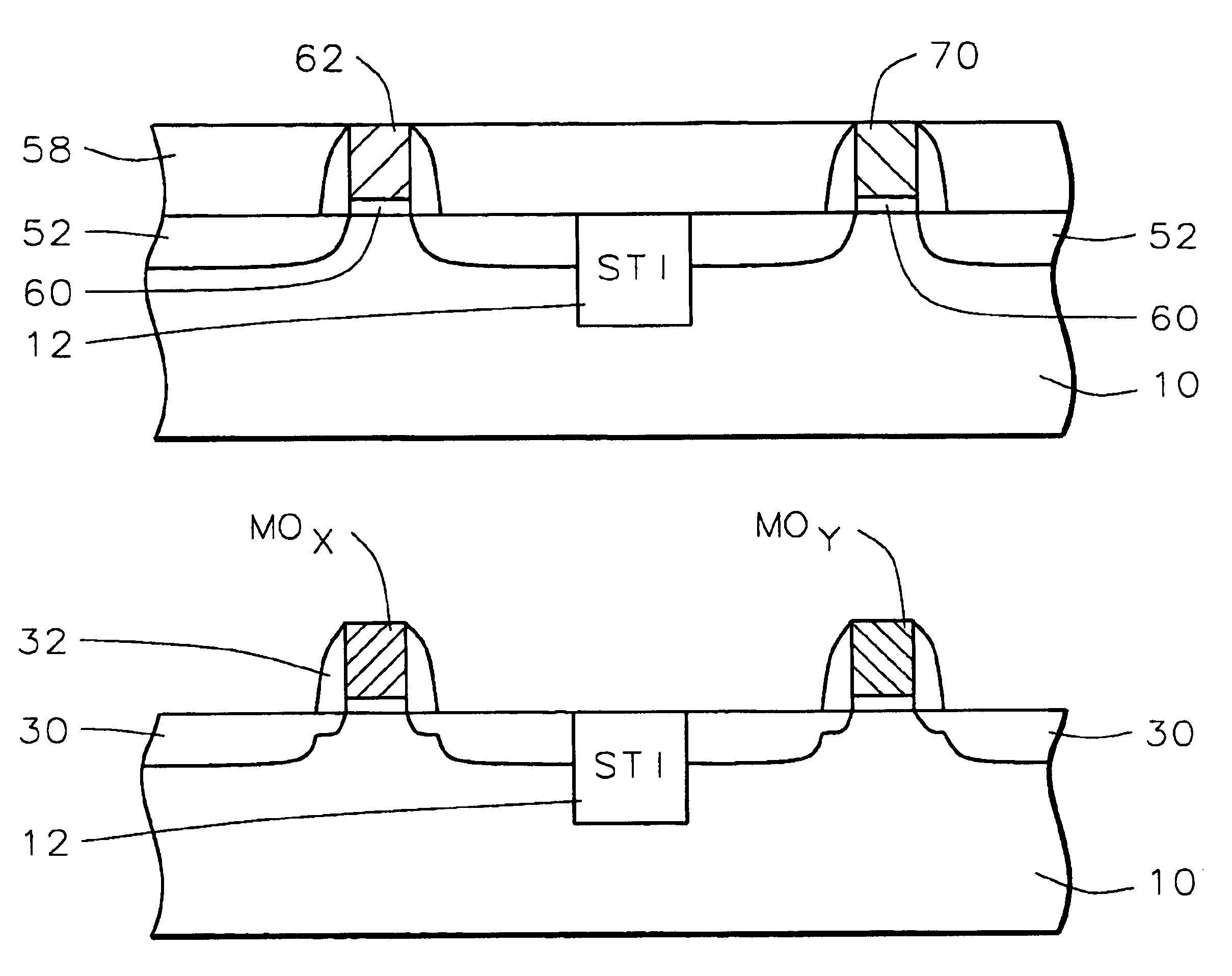
[0035]Now, the dual-metal gates of the present invention are to be formed. A gate dielectric layer 60 is deposited or thermally grown on the exposed substrate surface within the dummy gate openings to a thickness of between about 15 and 150 Angstroms, as shown in FIG. 8. As in the first embodiment, the dielectric layer may be a low dielectric constant material such as silicon dioxide, nitrided silicon dioxide, silicon nitride, or their combinations or a high dielectric constant gate dielectric material such as zirconium oxide, hafnium oxide, aluminum oxide, tantalum pentoxide, barium strontium titanates, and crystalline oxide.
[0036]Referring now to FIG. 9, a metal layer 62 is formed over the gate dielectric layer 60. The metal layer 62 may be formed by sputtering, evaporation, chemical vapor deposition (CVD), or electroplating. The deposited metal can be ruthenium, iridium, osmium, rhodium, rhenium, or similar metals. A CMP process polishes away the metal layer not within the dummy ...
second embodiment
[0044]As shown in FIG. 13, the damascene gate process described in the second embodiment can be used to form the two gate MOX and MOY. The gates will each be implanted with different dosages of oxygen ions to form these two metal oxide gates having different work functions.
[0045]In both FIGS. 12 and 13, the gate having the higher work function will be the PMOSFET and the gate having the lower work function will be the NMOSFET.
[0046]The process of the present invention provides three simple, manufacturable dual-metal gate processes. The conventional CMOS process flow is maintained. The work function of the gates is simply tuned by the oxidation process. The dual-metal gates comprise a metal and a metal oxide, or two metal oxides having different work functions. The metal oxide having the higher work function will be used for the PMOS gate and the metal oxide having the lower work function will be used for the NMOS gate.
PUM
 Abstract
Description
Claims
Application Information