Packaging method for substrate

一种封装方法、基板的技术,应用在有机半导体器件、电固体器件、半导体器件等方向,能够解决封装失败、框胶300胶高胶宽不均匀、框胶300胶高胶宽很难等问题,达到一致高度及宽度、封装效果好、制程简便的效果

Active Publication Date: 2016-07-27
TCL CHINA STAR OPTOELECTRONICS TECH CO LTD
View PDF5 Cites 12 Cited by
  • Summary
  • Abstract
  • Description
  • Claims
  • Application Information

AI Technical Summary

Problems solved by technology

In the packaging method of the above-mentioned substrate, since the sealant 300 does not contain spacer particles, it is difficult to control the height and width of the sealant 300 after the packaging cover plate 100 and the substrate 200 are combined, and different positions on the substrate 200 The adhesive height and adhesive width of the frame adhesive 300 may be uneven, resulting in poor sealing of the obtained substrate packaging structure, resulting in packaging failure

Method used


Image

  • Packaging method for substrate
  • Packaging method for substrate
  • Packaging method for substrate

Examples


Embodiment Construction

[0036] In order to further explain the technical means adopted by the present invention and its effects, the following describes in detail the preferred embodiments of the present invention and the accompanying drawings.

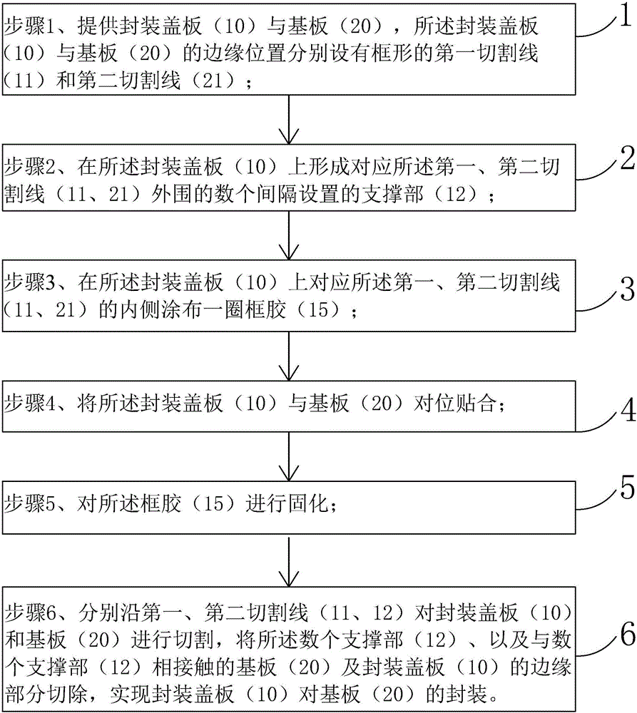
[0037] See figure 2 , The present invention provides a substrate packaging method, including the following steps:

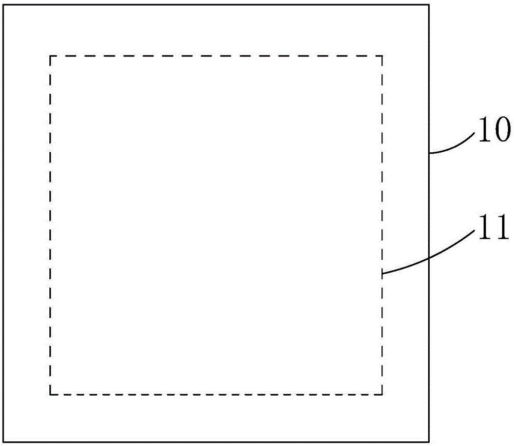
[0038] Step 1, such as image 3 with Figure 4 As shown, a package cover 10 and a substrate 20 to be packaged are provided. The edge of the package cover 10 is provided with a frame-shaped first cutting line (cutting line) 11, and the edge of the substrate 20 is provided with a frame-shaped The second cutting line 21.

[0039] Specifically, the packaging cover plate 10 is a glass plate.

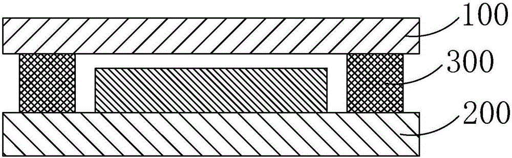
[0040] Specifically, the substrate 20 is an OLED substrate, including a TFT substrate 23 and an OLED device 25 provided on the TFT substrate 23, and the second cutting line 21 corresponds to the periphery of the OLED device 25 on the substrate 20.

[0041] Step 2, suc...


PUM


Abstract

The invention provides a packaging method for a substrate. Multiple supporting parts arranged at intervals are formed on the edge of a packaging cover plate; after the packaging cover plate is aligned to and fitted with the to-be-packaged substrate, the gap between the packaging cover plate and the substrate is limited; the height of seal without spacers is ensured; the width of the seal is ensured as well under a certain seal coating amount; in addition, the supporting parts, the substrate in contact with the supporting parts and the edge part of the packaging cover plate are cut after packaging, so that the substrate packaged by the seal without spacers is obtained; it is ensured that the seal has consistent height and width; and in addition, the packaging method is simple and convenient in process, and good in packaging effect.

Description

Technical field [0001] The present invention relates to the field of display technology, in particular to a method for packaging a substrate. Background technique [0002] In the field of display technology, flat panel display technologies (LCD, OLED) have gradually replaced CRT displays. Planar light source technology is a new type of light source, and its technology research and development has approached the level of market mass production. Among flat panel display and flat light source technologies, the bonding of two pieces of flat glass is a very important technology, and its sealing effect will directly affect the performance of the device. [0003] Ultraviolet light (UV) curing technology is the earliest and most commonly used technology for LCD / OLED packaging. It has the following characteristics: no solvent or a small amount of solvent is used, which reduces the pollution of solvents to the environment; low energy consumption, low-temperature curing, suitable for heat S...

Claims


Application Information

Patent Timeline
Patent Type & Authority Applications(China)
IPC IPC(8): H01L51/56H01L51/52
CPCH10K50/8426H10K71/00H10K50/841H10K71/851H10K50/80H10K50/84C03C25/6226C03C27/06
Inventor 刘亚伟
Owner TCL CHINA STAR OPTOELECTRONICS TECH CO LTD
Why Eureka
Try Eureka