Shifting register unit, gate driving circuit and display device

A technology for shift registers and gates, which is applied in the field of gate drive circuits, display devices, and shift register units, and can solve problems such as decreased stability of GOA circuits

Active Publication Date: 2015-05-27
BOE TECH GRP CO LTD
View PDF8 Cites 10 Cited by
  • Summary
  • Abstract
  • Description
  • Claims
  • Application Information

AI Technical Summary

Problems solved by technology

[0006] Embodiments of the present invention provide a shift register unit, a gate drive circuit, and a display device, which can solve the problem in the prior art that the stability of the GOA circuit decreases due to errors in the process of charging and discharging nodes.

Method used


Image

  • Shifting register unit, gate driving circuit and display device
  • Shifting register unit, gate driving circuit and display device
  • Shifting register unit, gate driving circuit and display device

Examples


Embodiment 1

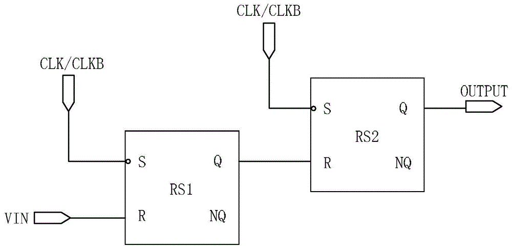
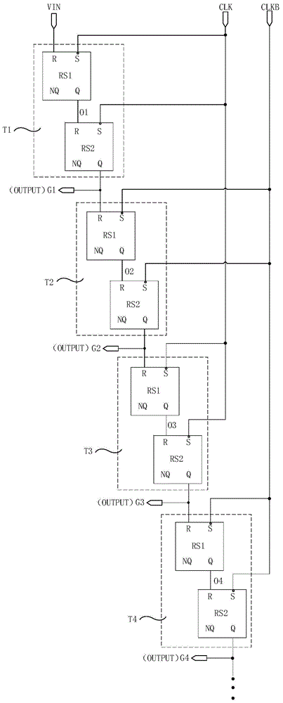
[0037] Such as figure 2 As shown, the first latch module RS1 or the second latch module RS2 may include:

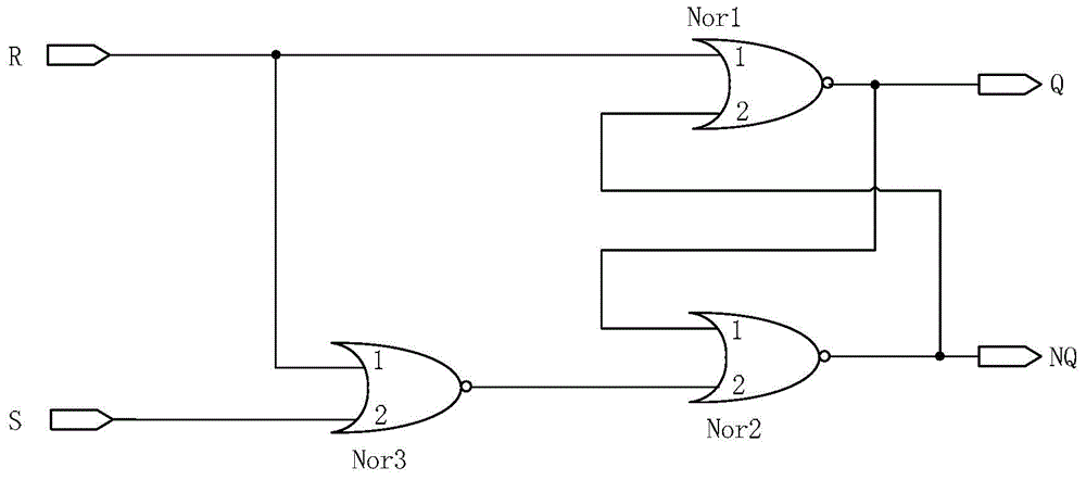
[0038] The first NOR gate nor1, the second NOR gate nor2 and the third NOR gate nor3.

[0039] Wherein, the first input terminal IN1 of the first NOR gate nor1 is used to receive the pulse signal, that is, the first input terminal IN1 of the first NOR gate nor1 can be connected to the first latch module RS1 or the second latch module RS2 The second input terminal R of the first NOR gate nor1; the second input terminal IN2 of the first NOR gate nor1 is connected to the output terminal of the second NOR gate nor2; the output terminal of the first NOR gate nor1 is connected with the first latch module RS1 or the second latch The output terminal Q of the storage module RS2 is connected.

[0040] The first input terminal IN1 of the second NOR gate nor2 is connected to the output terminal of the first NOR gate nor1; the second input terminal IN2 of the second NOR gate nor2 is ...

Embodiment 2

[0061] The first NOR gate nor1, the second NOR gate nor2 or the third NOR gate nor3, such as Figure 5 As shown, it may include: a first transistor M1, a second transistor M2, a third transistor M3 and a fourth transistor M4.

[0062] The gate of the first transistor M1 is connected to the first input terminal IN1 of the NOR gate (nor1, nor2 or nor3), the first pole is connected to the first voltage terminal VDDA, and the second pole is connected to the first pole of the second transistor M2 .

[0063] The gate of the second transistor M2 is connected to the second input terminal IN2 of the NOR gate (nor1, nor2 or nor3), and the second pole is connected to the output terminal OUT of the NOR gate;

[0064] The gate of the third transistor M3 is connected to the gate of the second transistor M2, the first pole is connected to the second pole of the second transistor M2, and the second pole is connected to the second voltage terminal GNDA.

[0065] The gate of the fourth transi...

Embodiment 3

[0080] The first NOR gate nor1, the second NOR gate nor2 or the third NOR gate nor3, such as Figure 6 As shown, it may include: a fifth transistor M5, a sixth transistor M6 and a seventh transistor M7.

[0081] Wherein, the gate of the fifth transistor M5 is connected to the first input terminal IN1 of the NOR gate (nor1, nor2 or nor3), the first pole is connected to the output terminal OUT of the NOR gate (nor1, nor2 or nor3), and the second pole is connected to the output terminal OUT of the NOR gate (nor1, nor2 or nor3). The second voltage terminal GNDA is connected to each other.

[0082] The gate of the sixth transistor M6 is connected to the second input terminal IN2 of the NOR gate (nor1, nor2 or nor3), the first pole is connected to the first pole of the fifth transistor M5, and the second pole is connected to the second voltage terminal GNDA. connect.

[0083] The gate and the first pole of the seventh transistor M7 are connected to the first voltage terminal VDDA,...


PUM


Abstract

The embodiment of the invention provides a shifting register unit, a gate driving circuit and a display device, relating to the technical field of display. According to the shifting register unit, the gate driving circuit and the display device, the problem that the stability of a GOA (Gate Driver on Array) circuit is decreased due to fault caused when a node is charged and discharged in the prior art can be solved. The shifting register unit comprises a first latch module and a second latch module, wherein a first input end of the first latch module is connected with a first clock signal end or a second clock signal end, a second input end is used for receiving pulse signals, and an output end of the first latch module is connected with a second input end of the second latch module; a first input end of the second latch module is connected with the first clock signal end or the second clock signal end, and an output end of the second latch module is connected with a signal output end of the shifting register unit; the first input ends of the first latch module and the second latch module are connected with a same signal end.

Description

technical field [0001] The invention relates to the field of display technology, in particular to a shift register unit, a gate drive circuit and a display device. Background technique [0002] Liquid Crystal Display (LCD for short) has the advantages of low radiation, small size and low power consumption, and is widely used in electronic products such as notebook computers, flat-screen TVs or mobile phones. A liquid crystal display is made up of pixel units arranged in a matrix. When the liquid crystal display is displayed, the data drive circuit can lock the input display data and clock signal timing sequence, convert it into an analog signal and input it to the data line of the liquid crystal panel, and the gate drive circuit can shift the input clock signal The bit registers are converted into voltages that control the on / off of pixels, and are applied to the gate lines of the liquid crystal panel row by row. [0003] In order to further reduce the production cost of l...

Claims


Application Information

Patent Timeline
Patent Type & Authority Applications(China)
IPC IPC(8): G09G3/36G11C19/28
CPCG09G3/3677G09G2310/0286G09G2310/08G09G2330/021G11C19/287
Inventor 宋琛吴仲远曹昆解红军
Owner BOE TECH GRP CO LTD
Why Eureka
Try Eureka