

Display substrate, manufacturing method of display substrate and liquid crystal display device
A display substrate and manufacturing method technology, applied in optics, instruments, electrical components, etc., can solve problems such as poor panel cutting and breaking, and achieve the effects of overcoming bad breaking, avoiding uneven distribution of sealing glue, and ensuring glue width
- Summary
- Abstract
- Description
- Claims
- Application Information
AI Technical Summary
Problems solved by technology
Method used
Image

Examples
Embodiment Construction
[0020] In order to make the object, technical solution and advantages of the present invention clearer, the implementation manner of the present invention will be further described in detail below in conjunction with the accompanying drawings.
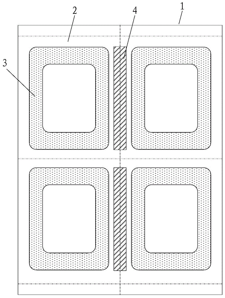
[0021] The display substrate 1 provided by the embodiment of the present invention, such as figure 1 As shown, it includes: at least one substrate area 2 to be cut arranged in an array.
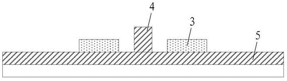
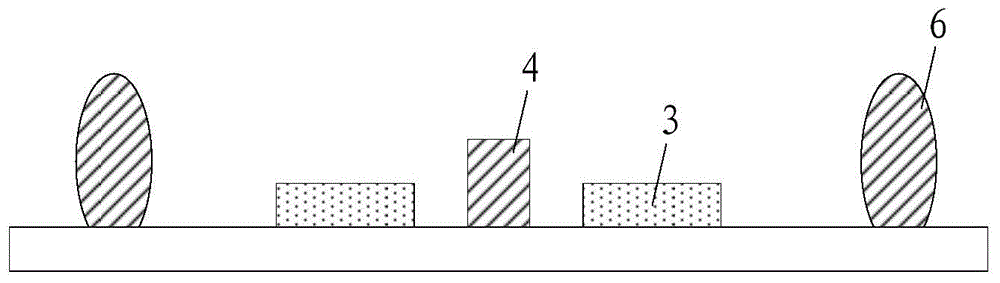
[0022] On the surface of the display substrate 1 , a sealant 3 is coated around the region of the substrate 2 to be cut, and a retaining wall 4 for blocking the sealant is arranged between adjacent regions of the substrate 2 to be cut.
[0023] The display substrate provided by the embodiment of the present invention includes at least one substrate region to be cut arranged in an array; on the surface of the display substrate, a sealant is coated around the substrate region to be cut, and is arranged between adjacent substrate regions to be cut. Ther...
PUM
| Property | Measurement | Unit |
|---|---|---|
| width | aaaaa | aaaaa |
Abstract
Description
Claims
Application Information