Method for improving prepared thin film thickness in rotary coating method
A thin-film thickness and spin-coating technology, which can be used in photo-engraving process coating equipment, devices for coating liquids on surfaces, coatings, etc.
- Summary
- Abstract
- Description
- Claims
- Application Information
AI Technical Summary
Problems solved by technology
Method used
Image
Examples
Embodiment Construction
[0018] The present invention will be further described below in conjunction with the accompanying drawings and embodiments.
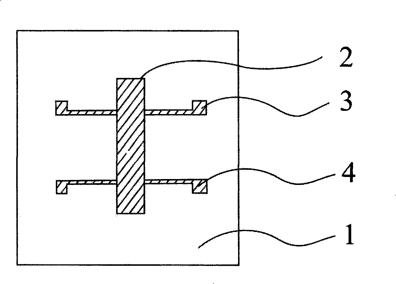
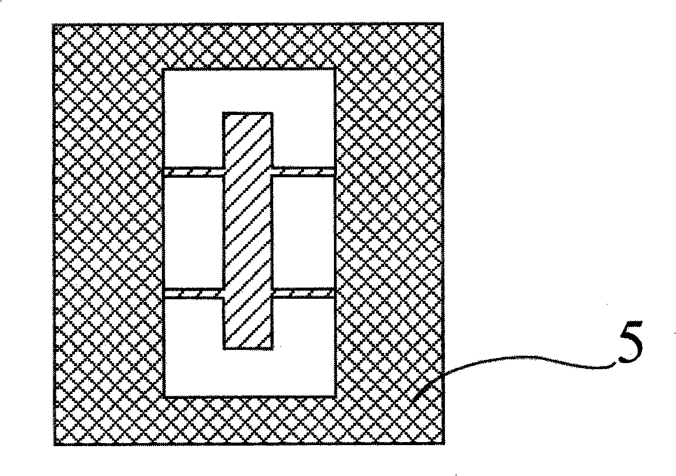
[0019] Taking the preparation of Love wave waveguide thin film as an example, a method of preparing thin film by spin coating method proposed in this paper is described. The Love wave device is divided into upper and lower layers in structure: the bottom layer is a piezoelectric wafer, the middle layer is an electrode, and the top layer is a waveguide film. The electrodes usually consist of a pair of interdigital transducers (IDTs), which may also contain reflective grids. Such as figure 1 As shown, the PMMA waveguide film will be prepared on the electrode 2, and the thickness of the PMMA waveguide film needs to reach about 2 μm, for which the frame spin coating process of the present invention is adopted.
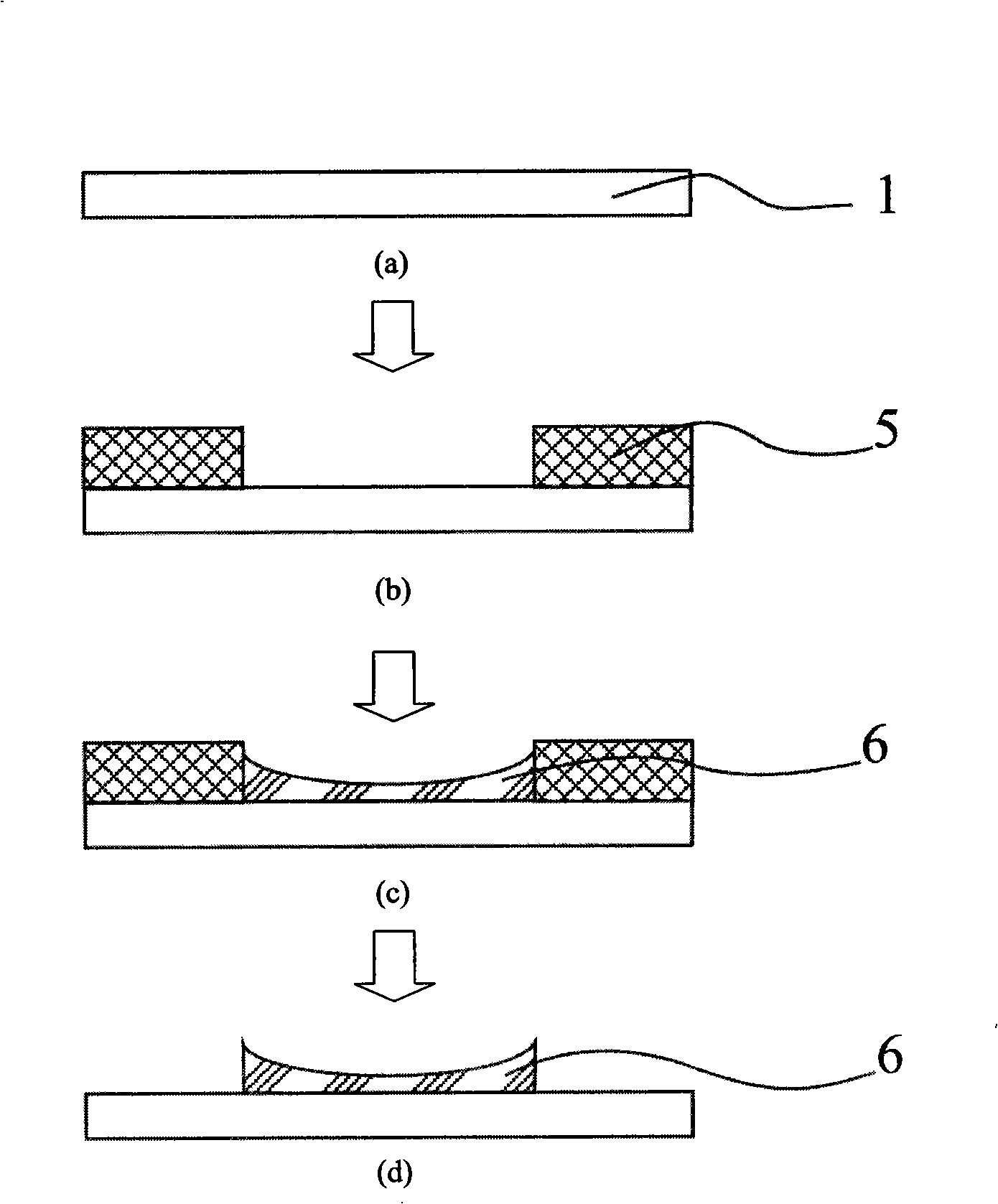
[0020] A kind of spin coating method provided by the present invention prepares the method for thin film as follows (example):
[0021] Accordin...
PUM
| Property | Measurement | Unit |
|---|---|---|
| Height | aaaaa | aaaaa |
Abstract
Description
Claims
Application Information


