

An electrostatic chuck and semiconductor processing device
An electrostatic chuck and substrate technology, which is applied in semiconductor/solid-state device manufacturing, circuits, discharge tubes, etc., can solve the problems of adverse effects of etching machine etching uniformity, prone to tilting, wafer tilting, etc., to improve process quality and process efficiency, reducing the probability of inclination, and reducing the cost of thimbles
- Summary
- Abstract
- Description
- Claims
- Application Information
AI Technical Summary
Problems solved by technology
Method used
Image

Examples
Embodiment 1
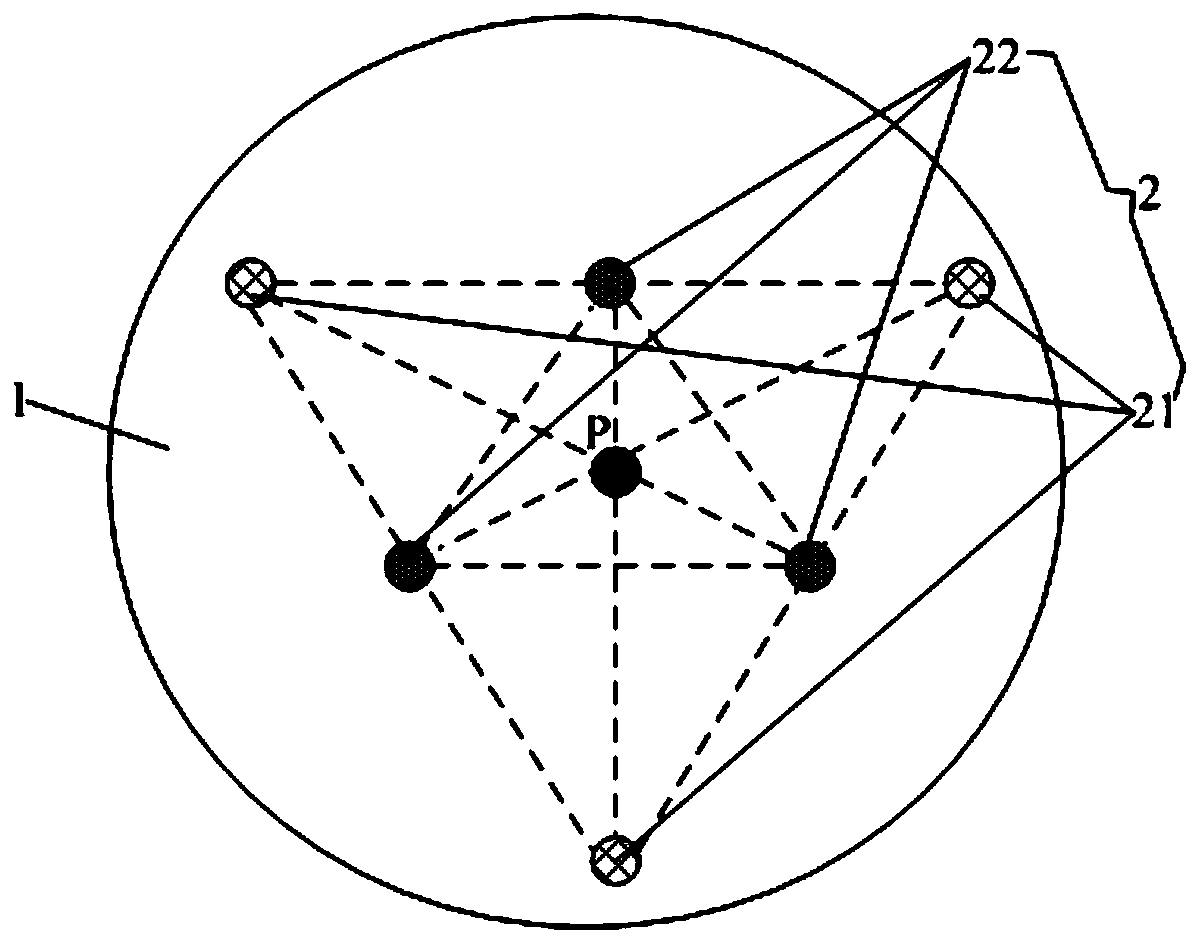
[0034] This embodiment provides an electrostatic chuck, such as figure 1 As shown, it includes an electrostatic chuck base 1 and a thimble assembly arranged inside the electrostatic chuck base 1. The thimble assembly can be raised and lowered to lift and lower the wafer placed on the electrostatic chuck base 1. The thimble assembly includes The thimbles 2 arranged in the edge area and the central area of the electrostatic chuck base 1 are distributed in a regular triangle of different sizes, and the center of the regular triangle coincides with the center P of the electrostatic chuck base 1 correspondingly.
[0035] By making the thimble 2 be arranged on the edge area and the central area of the electrostatic chuck base body 1 to form a regular triangle distribution of different sizes, and make the center of the regular triangle coincide with the center P of the electrostatic chuck base body 1 correspondingly, it is possible to place the electrostatic chuck on the wafer rel...
Embodiment 2
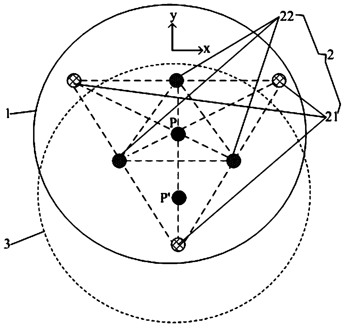
[0046] This embodiment provides an electrostatic chuck, which is different from Embodiment 1, such as Image 6 As shown, the three second thimbles 22 are respectively located inside the sides of the regular triangle formed by the three first thimbles 21 and correspond to the midpoints of the sides of the regular triangle formed by the first thimbles 21 .
[0047] Arranged in this way, the first thimbles 21 form an equilateral triangle distribution in the edge area of the electrostatic chuck base 1, and the second thimbles 22 form an equilateral triangle distribution in the central area of the electrostatic chuck base 1, so that the relative static electricity on the wafer can be formed. When the center of gravity of the chuck base 1 shifts within a certain range, the rest of the thimble 2 that effectively supports the wafer can still effectively disperse the force applied to the wafer, so that the gravity of the wafer is still equal to that of the thimble 2 that effectively...
Embodiment 3
[0050] This embodiment provides an electrostatic chuck, which is different from Embodiment 1-2, such as Figure 7 As shown, the three second thimbles 22 are respectively located outside the sides of the regular triangle formed by the three first thimbles 21 and correspond to the midpoints of the sides of the regular triangle formed by the first thimbles 21 .
[0051] Arranged in this way, the first thimbles 21 form an equilateral triangle distribution in the edge area of the electrostatic chuck base 1, and the second thimbles 22 form an equilateral triangle distribution in the central area of the electrostatic chuck base 1, so that the relative static electricity on the wafer can be formed. When the center of gravity of the chuck base 1 shifts within a certain range, the remaining thimbles that effectively support the wafer can still effectively disperse the force applied to the wafer, so that the gravity of the wafer is still equal to the resultant force of the thimble 2 t...
PUM
 Abstract
Description
Claims
Application Information