Circuit board perforating mechanism capable of carrying out marking

A circuit board and punch technology, which is applied in printing, stamping, metal processing, etc., can solve the problem that the circuit board production process and marking program cannot be carried out at the same time, waste manpower and economic costs, and reduce the risk of counterfeit production Risk, improved operational reliability, low production cost

Pending Publication Date: 2018-03-16
SHANGHAI NCATEST TECH CO LTD
View PDF10 Cites 1 Cited by
  • Summary
  • Abstract
  • Description
  • Claims
  • Application Information

AI Technical Summary

Problems solved by technology

However, the actual situation is that the production process of the circuit board and the marking process cannot be carried out at the same time, which greatly wastes manpower and economic costs.

Method used


Image

  • Circuit board perforating mechanism capable of carrying out marking

Examples


Embodiment Construction

[0012] The present invention will be further described below in conjunction with specific examples.

[0013] The present invention will be described in detail below in conjunction with specific embodiments shown in the accompanying drawings. However, these embodiments do not limit the present invention, and any structural, method, or functional changes made by those skilled in the art according to these embodiments are included in the protection scope of the present invention.

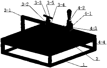
[0014] The application principle of the present invention will be further described below in conjunction with the accompanying drawings and specific embodiments. as attached figure 1 As shown, the circuit board punching mechanism capable of marking includes a base 1, the base 1 is provided with a base plate 2, and the base plate 2 is fixedly provided with a punching device 3 and a marking device 4. The hole device 3 and the marking device 4 are distributed at 90 degrees. The punch device 3 includes a...


PUM


Abstract

The invention discloses a circuit board perforating mechanism capable of carrying out marking. The problem of perforating a circuit board is solved, the problem how to mark the circuit board in the circuit board production process is also solved, by arranging a marking device, different types of label seals can be printed on the circuit board, the anti-fake degree of the circuit board is improved,the risk that the circuit board is counterfeited by other factories is reduced, moreover, the whole operation is easy, precision is high, the manufacturing cost is low, the effect is enhanced remarkably, and the overall high efficiency and operation reliability are also improved.

Description

technical field [0001] The invention relates to the fields of punching holes and anti-counterfeiting of circuit boards, and more specifically relates to a punching mechanism for circuit boards capable of marking. Background technique [0002] The circuit board is an important electronic component, a support for electronic components, and a carrier for the electrical connection of electronic components, which plays a very important role. In the process of circuit board production and use, the punching process is an indispensable process, and looking at the current market, each semiconductor manufacturer cherishes the fruits of their labor, and the anti-counterfeiting awareness has been significantly improved, so each semiconductor manufacturer in their own production The circuit board will be marked with its own anti-counterfeiting mark to prevent counterfeiting. However, the actual situation is that the production process procedure and the marking procedure of the circuit b...

Claims


Application Information

Patent Timeline
Patent Type & Authority Applications(China)
IPC IPC(8): B26F1/24B26D5/10B41K3/04
CPCB26D5/10B26F1/24B41K3/04
Inventor 胡忠臣
Owner SHANGHAI NCATEST TECH CO LTD
Why Eureka
Try Eureka