

Concentrating flux plate and device transfer equipment
A technology of transfer device and magnetic plate, which is applied in semiconductor/solid-state device manufacturing, electrical components, circuits, etc., can solve problems such as time-consuming and low efficiency, and achieve the effect of improving manufacturing efficiency
- Summary
- Abstract
- Description
- Claims
- Application Information
AI Technical Summary
Problems solved by technology
Method used
Image

Examples
Embodiment Construction
[0023] The word "embodiment" as used in this specification means an example, instance or illustration. Furthermore, as used in this specification and the appended claims, the article "a" or "an" may generally be construed as "one or more" unless specified otherwise or clear from the context in the singular.
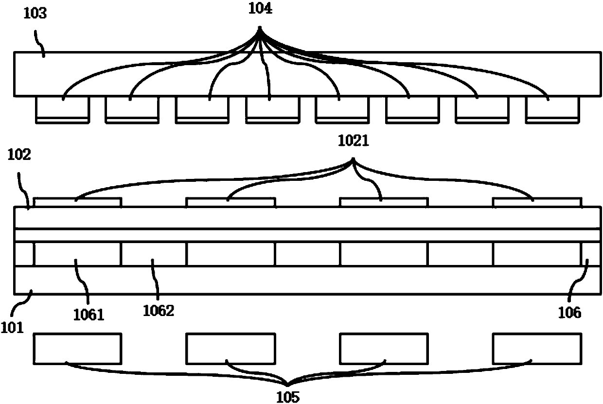
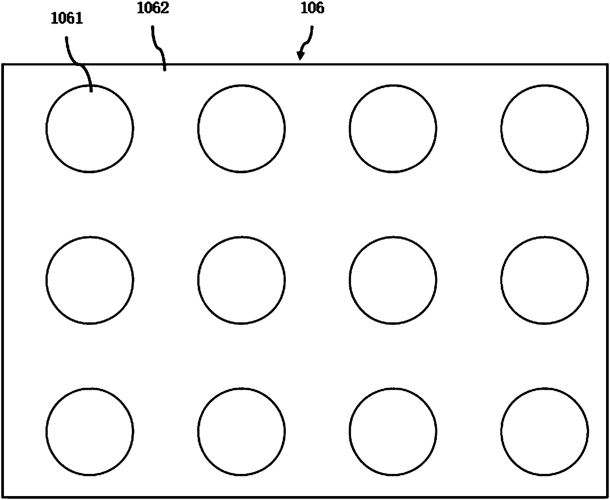
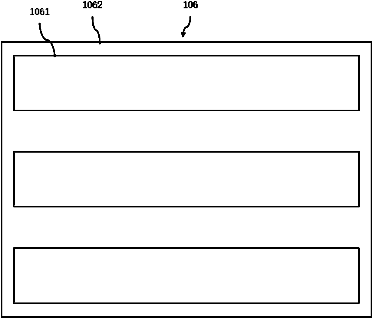
[0024] refer to figure 1 , figure 2 with image 3 , figure 1 It is a schematic diagram of the positional relationship between the device transfer device provided with the magnetic conductive plate 106 and the array substrate 102 on which the device 104 is to be provided in the present invention, figure 2 It is a schematic diagram of the first embodiment of the magnetic conductive plate 106 of the present invention, image 3 It is a schematic diagram of the second embodiment of the magnetically conductive plate 106 of the present invention.
[0025] The magnetically conductive plate 106 of the present invention can be disposed in the device transfer device.
[0026...
PUM
 Abstract
Description
Claims
Application Information