

Micro device transfer equipment, method for transferring micro devices by adopting same and micro device transfer board
A transfer device and transfer plate technology, which is applied in the direction of instruments, nonlinear optics, optics, etc., can solve the problems of time-consuming and low efficiency, and achieve the effect of improving manufacturing efficiency
- Summary
- Abstract
- Description
- Claims
- Application Information
AI Technical Summary
Problems solved by technology
Method used
Image

Examples
Embodiment Construction
[0024] The word "embodiment" as used in this specification means an example, instance or illustration. Furthermore, as used in this specification and the appended claims, the article "a" or "an" may generally be construed as "one or more" unless specified otherwise or clear from the context in the singular.
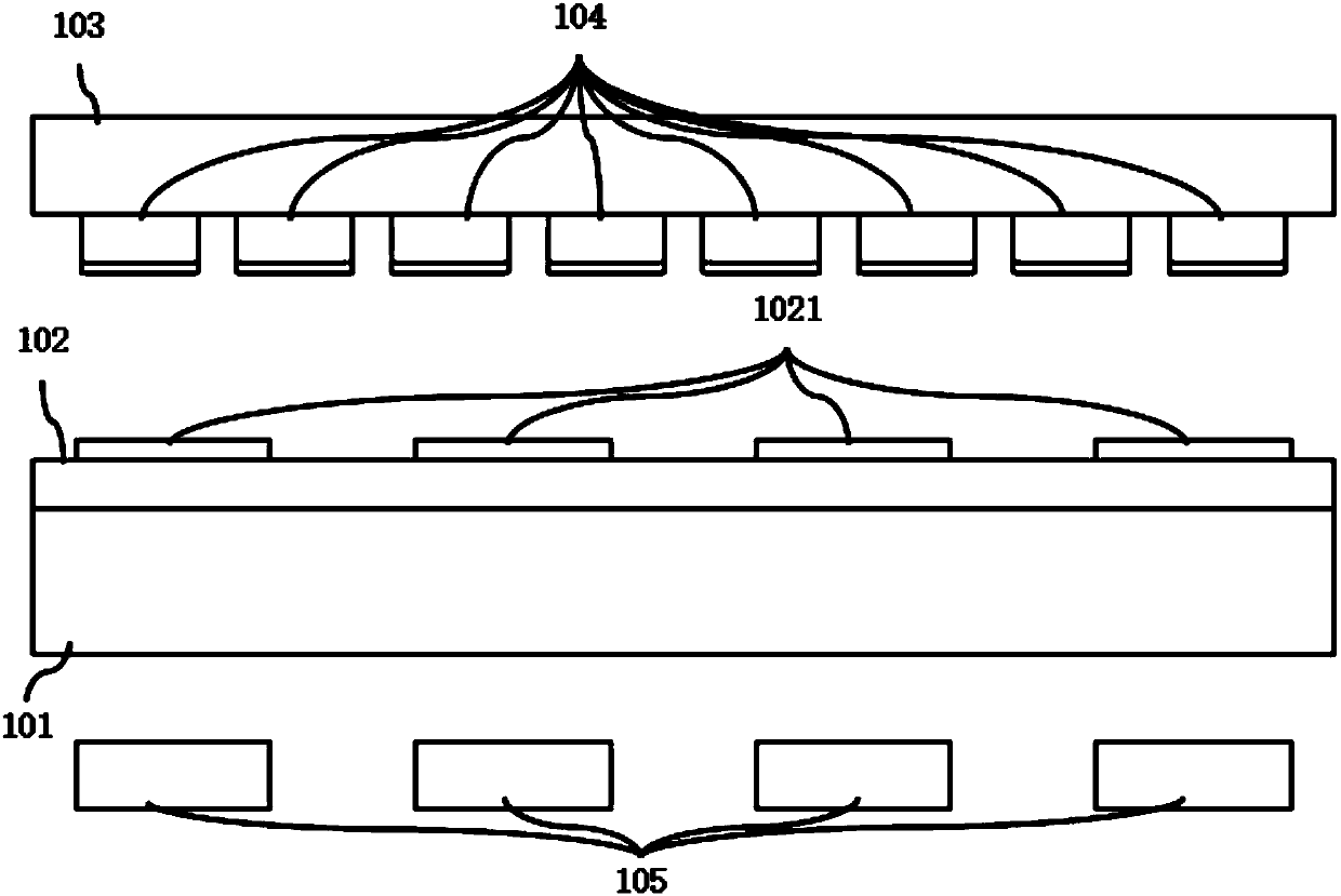
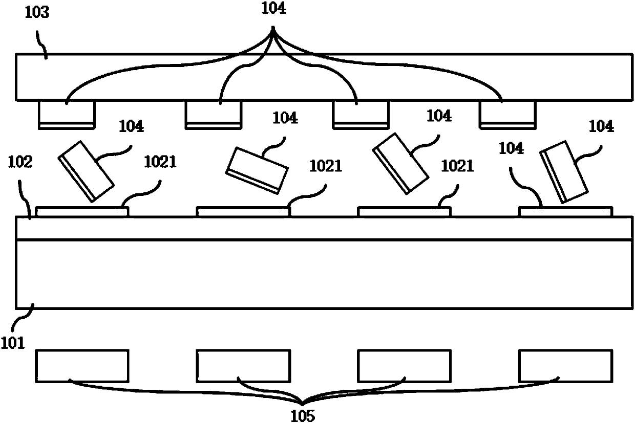
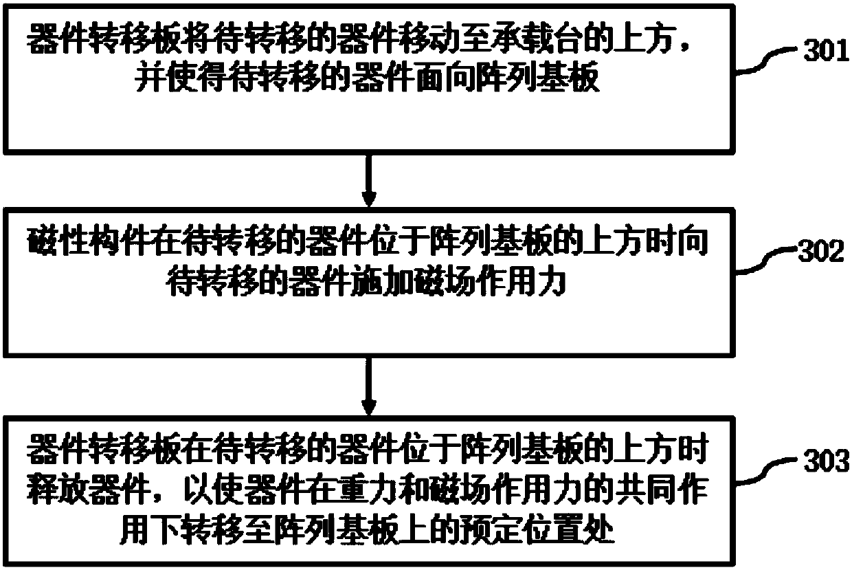
[0025] refer to figure 1 and figure 2 , figure 1 is a schematic diagram of the positional relationship between the device transfer device of the present invention and the array substrate 102 on which the device 104 is to be placed, figure 2 It is a schematic diagram of the process of transferring the device 104 to the array substrate 102 by the device transferring device of the present invention.
[0026] The device transfer device of the present invention includes a carrier platform 101 , a device transfer plate 103 and a magnetic member 105 . The device (Micro Device) 104 of the present invention can be, for example, a Micro Light Emitting Diode (Micro LED).
[0...
PUM
 Abstract
Description
Claims
Application Information