Light emitting element and method of making same

a technology of light emitting elements and methods, applied in the direction of polycrystalline material growth, chemistry apparatus and processes, crystal growth process, etc., can solve the problems of micro-pipe defects penetrating vertically, light emitting elements employing sic substrates, and poor crystalline quality of sic single crystal wafers, etc., to achieve good manufacturing efficiency

Inactive Publication Date: 2008-01-15
KOHA CO LTD
View PDF8 Cites 18 Cited by
  • Summary
  • Abstract
  • Description
  • Claims
  • Application Information

AI Technical Summary

Benefits of technology

[0011]It is another object of the invention to provide a light emitting element with a good manufacturing efficiency and a method of making the same.

Problems solved by technology

However, there is a serious problem in the light emitting element employing the SiC substrate.
The SiC single crystal wafer has a bad crystalline quality such that there exist micro-pipe defects penetrating vertically in the SiC single crystal wafer.
This causes a bad efficiency in the manufacture of light emitting element.
Thus, ultraviolet light cannot be outputted from the substrate side.

Method used


Image

  • Light emitting element and method of making same
  • Light emitting element and method of making same
  • Light emitting element and method of making same

Examples


example 1

Forming of n-GaN Thin Film on P-type Conductivity Substrate

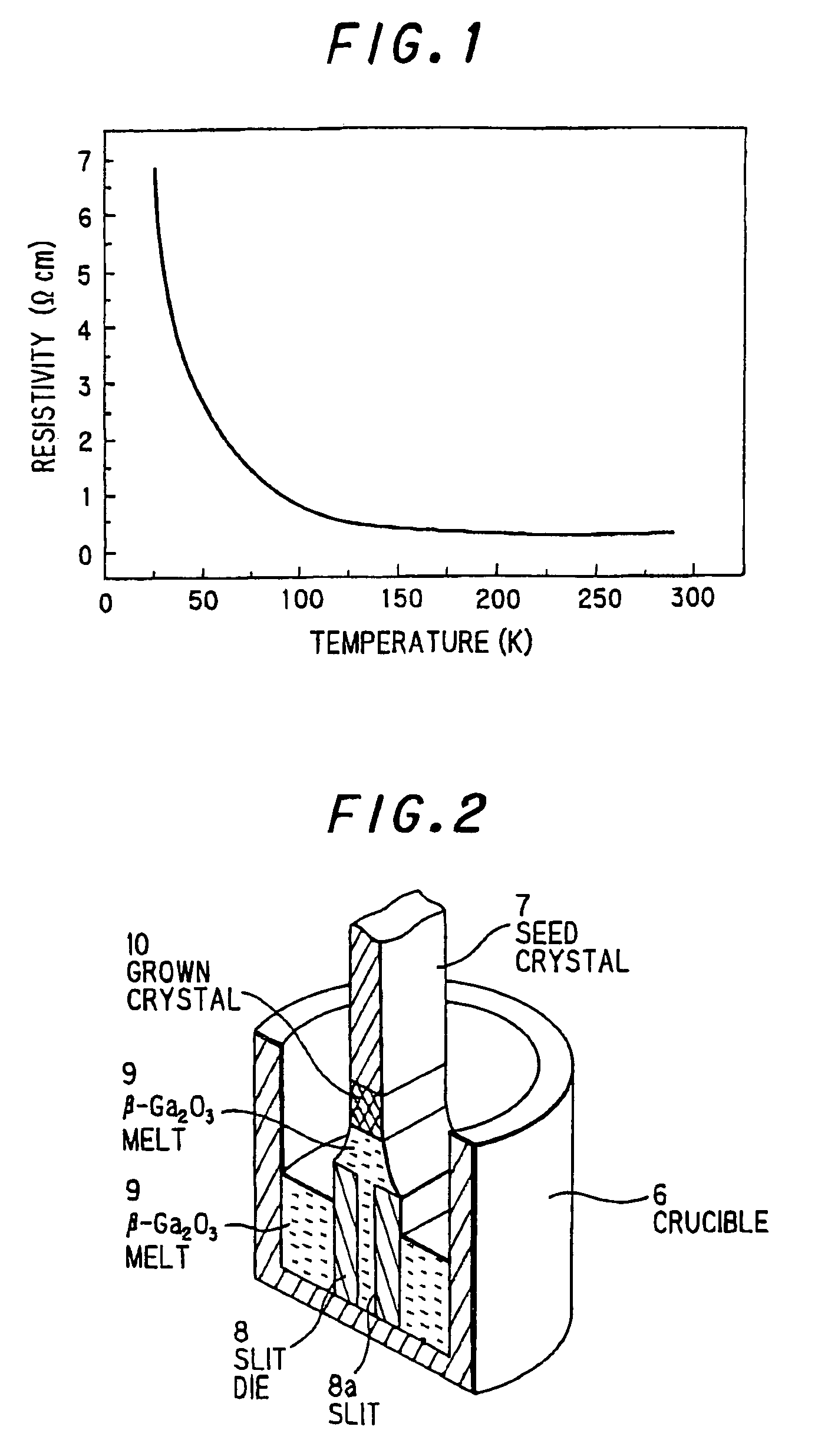
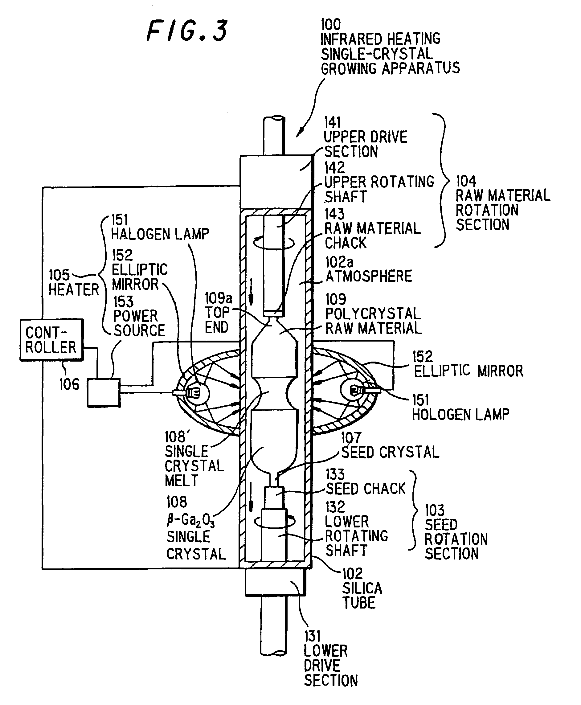
[0088]The p-type conductivity substrate is made as follows. First, β-Ga2O3 single crystal is prepared by FZ method. The β-Ga2O3 polycrystalline raw material is obtained by uniformly mixing, for example, β-Ga2O3 including MgO (p-dopant source) and charging a predetermined amount of the mixture into a rubber tube, cold-compressing it at 500 MPa to form a stick, then sintering it at 1500° C. for ten hours in the atmosphere. Thereby, β-Ga2O3 system polycrystalline raw material including Mg is obtained. By another way, β-Ga2O3 seed crystal is provided. Under the growth atmosphere with total pressure of 1 to 2 atm, flowing mixture gas of N2 and O2 at 500 ml / min, the β-Ga2O3 seed crystal and β-Ga2O3 system polycrystalline raw material are contacted to each other in the silica tube, and they are heated such that the β-Ga2O3 seed crystal and β-Ga2O3 system polycrystalline raw material are melted at the contacting portion. The meltin...

example 2

Light Emitting Element with pn-junction

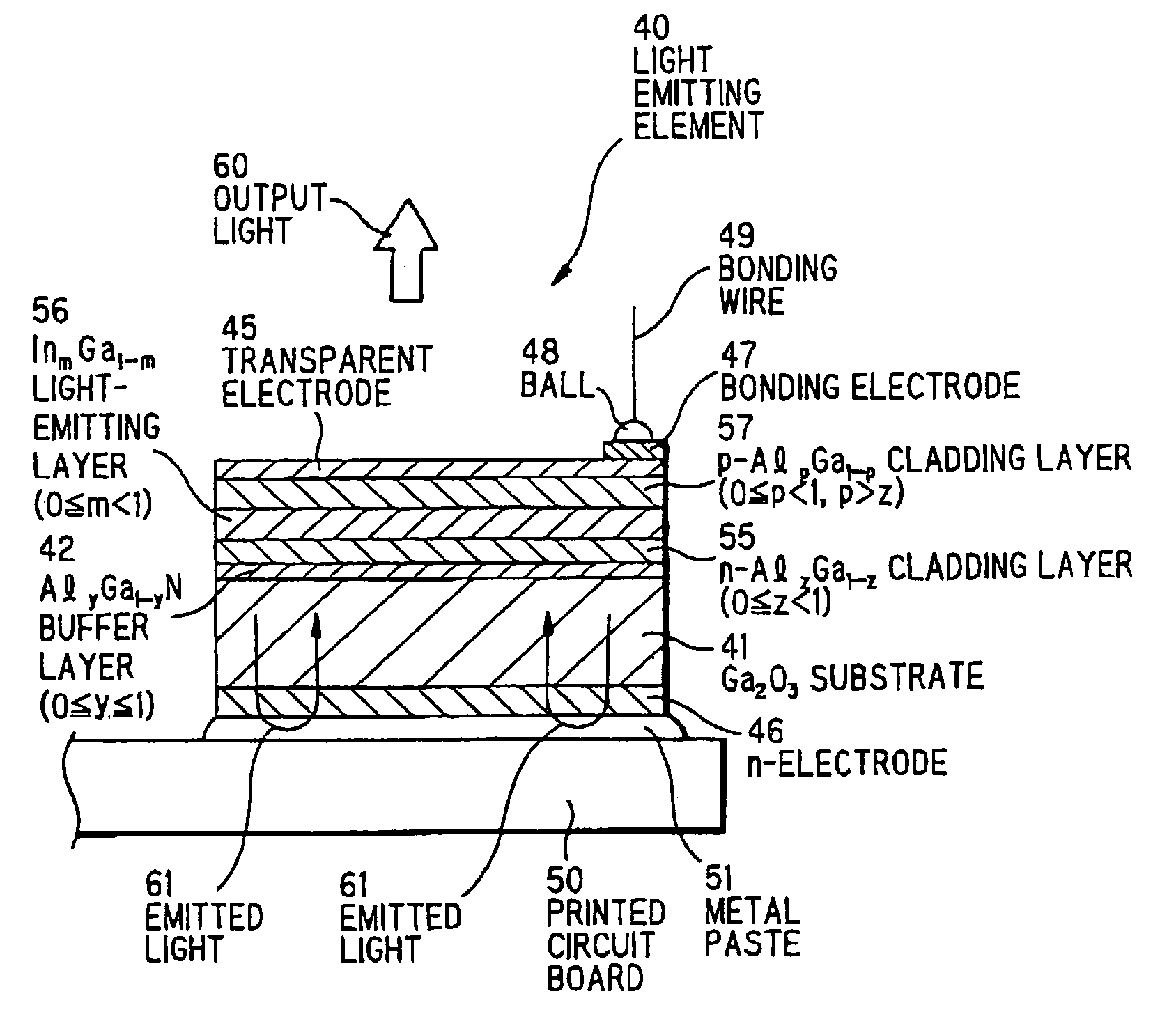
[0090]FIG. 9 shows a light emitting element with pn-junction mounted on a printed circuit board. The light emitting element 40 includes: a Ga2O3 substrate 41 of β-Ga2O3 single crystal; a AlXGa1−XN buffer layer 42 (0≦x≦1) formed on the Ga2O3 substrate 41; a n-GaN layer 43 formed on the AlXGa1−XN buffer layer 42; a p-GaN layer 44 formed on the n-GaN layer 43; a transparent electrode 45 formed on the p-GaN layer 44; a Au bonding electrode 47 formed on part of the transparent electrode 45; and a n-electrode 46 formed on the bottom surface of the Ga2O3 substrate 41. The light emitting element 40 is mounted on the printed circuit board 50 through a metal paste 51 and a bonding wire 49 is bonded to the bonding electrode 47 while forming a ball 48.

[0091]The light emitting element 40 emits light at the pn-junction interface where the n-GaN layer 43 and p-GaN layer 44 are bonded. Emitted light is output such that part of emitted light is output, as outp...

example 3

Flip-chip Type Light Emitting Element

[0092]FIG. 10 shows a flip-chip type light emitting element. The light emitting element 40 includes: a Ga2O3 substrate 41 of β-Ga2O3 single crystal; a AlXGa1−XN buffer layer 42 (0≦x≦1) formed on the Ga2O3 substrate 41; a n-GaN layer 43 formed on the AlXGa1−XN buffer layer 42; a p-GaN layer 44 formed on part of the n-GaN layer 43; a n-electrode 46 formed on the n-GaN layer 43; and a p-electrode 52 formed on the p-GaN layer 44. The light emitting element 40 is flip-chip bonded through solder balls 63, 64 beneath the p-electrode 52 and n-electrode 46 to lead frames 65, 66.

[0093]The light emitting element 40 emits light at the pn-junction interface where the n-GaN layer 43 and p-GaN layer 44 are bonded. Emitted light is output, as output light 60, upward transmitting through the Ga2O3 substrate 41.


PUM

PropertyMeasurementUnit
resistivityaaaaaaaaaa
wavelengthaaaaaaaaaa

Abstract

A light emitting element has a substrate of gallium oxides and a pn-junction formed on the substrate. The substrate is of gallium oxides represented by: (AlXInYGa(1−X−Y))2O3 where 0≦x≦1, 0≦y≦1 and 0≦x+y≦1. The pn-junction has first conductivity type substrate, and GaN system compound semiconductor thin film of second conductivity type opposite to the first conductivity type.

Description

STATEMENT OF RELATED APPLICATIONS[0001]This application is based on Japanese patent application Nos. 2003-137912 and 2002-160630, the entire contents of which are incorporated herein by reference. Also, the present application is a continuation of U.S. patent application Ser. No. 10 / 452,158 filed May 30, 2003, now U.S. Pat. No. 6,977,397, granted on Dec. 30, 2005.BACKGROUND OF THE INVENTION[0002]1. Field of the Invention[0003]This invention relates to a light emitting element with a wide bandgap enough to emit visible light to ultraviolet light and a method of making the same, and relates particularly to a light emitting element employing a colorless, transparent and conductive substrate that transmits emit visible light to ultraviolet light, offering a vertical structure in electrode configuration, and allowing emitted light to be outputted from the substrate side and a method of making the same.[0004]2. Description of the Related Art[0005]Conventionally, a light emitting element w...

Claims


Application Information

Patent Timeline
Patent Type & Authority Patents(United States)
IPC IPC(8): H01L33/00C30B15/00C30B15/34H01L21/205H01L33/28H01L33/32H01L33/40
CPCC30B15/00C30B29/16H01L21/02425H01L21/02458H01L21/0254H01L21/0256H01L21/02576H01L21/02579H01L21/0262H01L33/0066H01L33/32C30B15/34H01L33/0025H01L33/42H01L33/62H01L2224/73265H01L33/007H01L2224/48463H01L2224/16245H01L2224/32225H01L2224/06102
Inventor ICHINOSE, NOBORUSHIMAMURA, KIYOSHIKANEKO, YUKIOGARCIA VILLORA, ENCARNACION ANTONIAAOKI, KAZUO
Owner KOHA CO LTD
Why Eureka
Try Eureka