Active area structure and formation method therefor

An active area and active layer technology, applied in semiconductor devices, electrical components, transistors, etc., can solve problems such as damage and unstable operation of memory cells, and achieve the effect of avoiding damage

Active Publication Date: 2018-03-20
UNITED MICROELECTRONICS CORP +1
View PDF2 Cites 15 Cited by
  • Summary
  • Abstract
  • Description
  • Claims
  • Application Information

AI Technical Summary

Problems solved by technology

In order to increase the memory capacity, the size of the storage unit of the memory needs to be reduced, but a large reduction in the size of the storage unit will cause other problems, making the operation of the storage unit unstable or damaged

Method used


Image

  • Active area structure and formation method therefor
  • Active area structure and formation method therefor
  • Active area structure and formation method therefor

Examples


Embodiment Construction

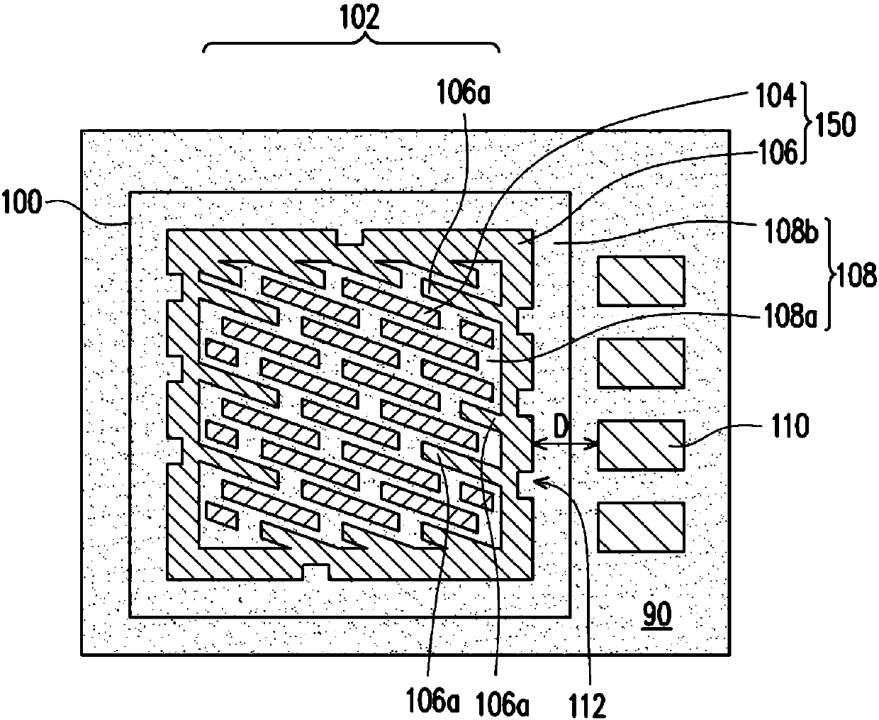
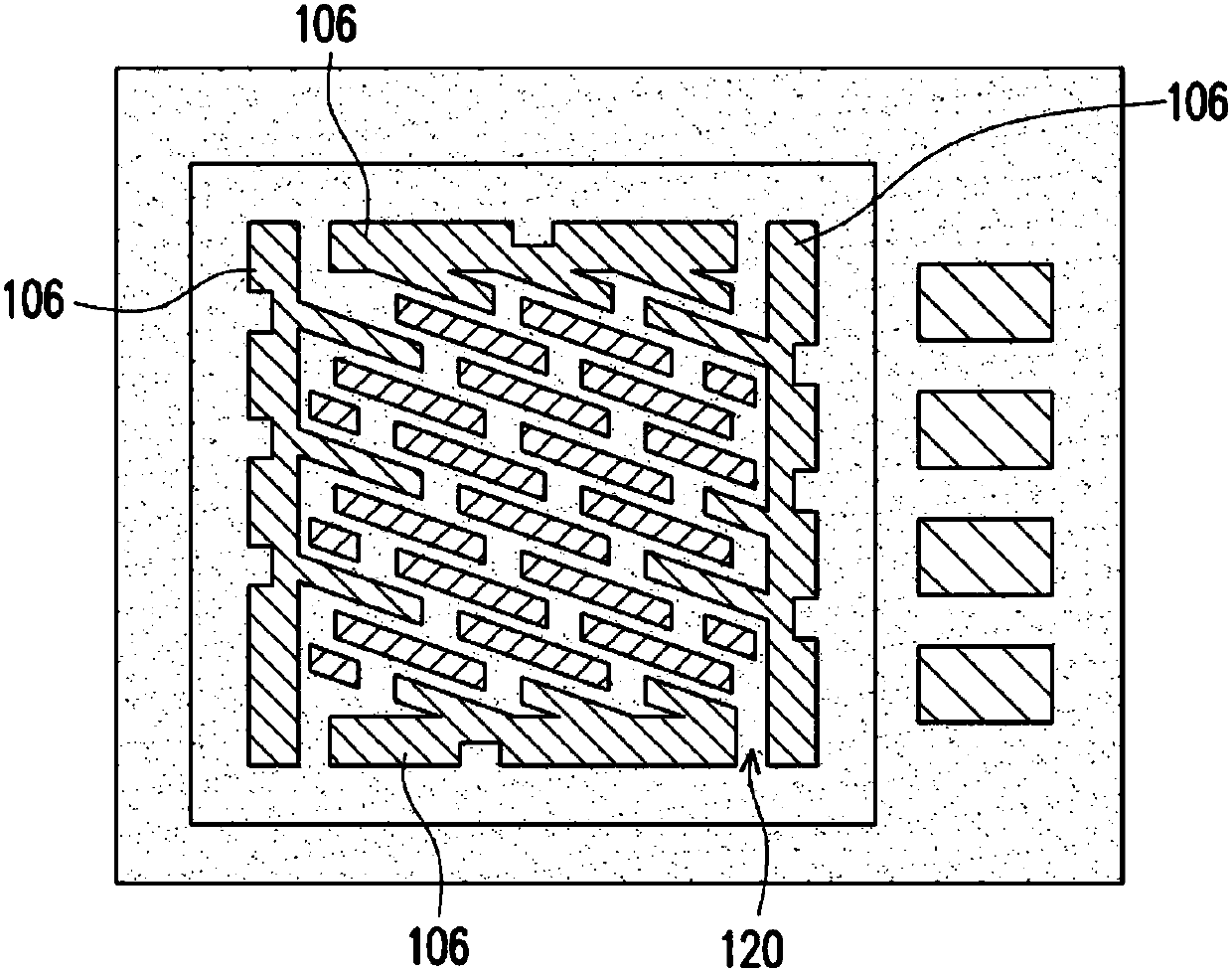
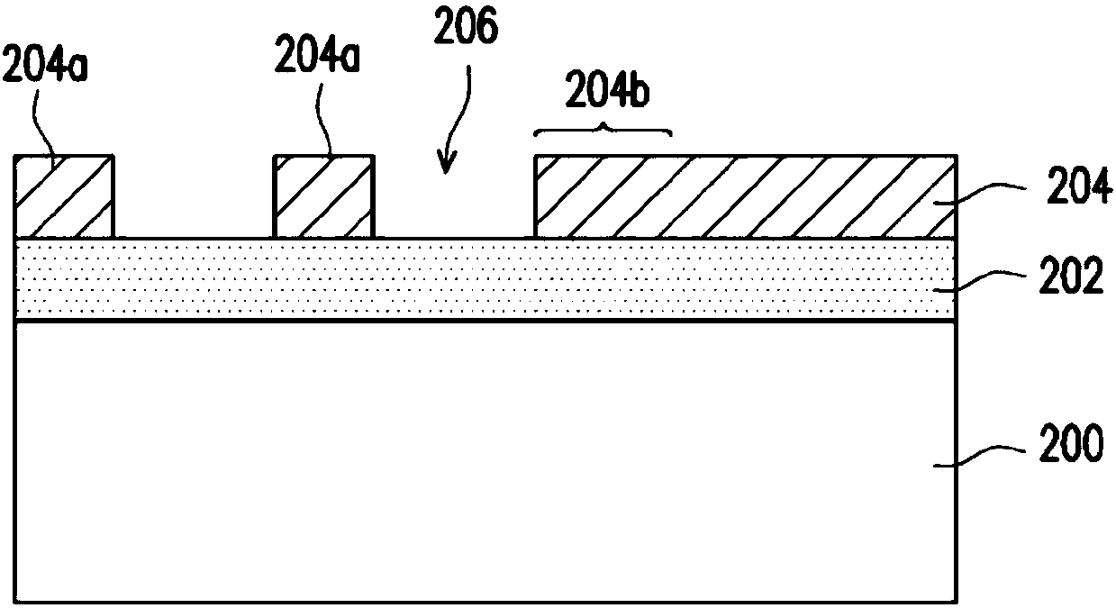
[0050] Semiconductor elements, such as memory cells, need to be isolated to achieve the effect of insulation, and the insulating structure is formed between these element units and between these elements under the requirement of high element density, for example, by means of a shallow trench insulation layer. Between the unit and the surrounding active area to provide insulation between components.

[0051] The invention considers the insulation quality between components and proposes a corresponding design.

[0052] The material of the shallow trench insulation layer is a dielectric material, and the element unit and the peripheral active area are formed by a part of the substrate, such as the surface layer of the silicon substrate, which is formed after patterning. Furthermore, the distance between the element units and the peripheral active area is larger than the gap between these element units, and occupying a larger area produces greater stress. Therefore, the material ...


PUM


Abstract

The invention discloses an active area structure and a formation method therefor. The active area structure comprises an element area, an active layer and a shallow trench insulating layer. The element area is defined on a substrate. The active layer is formed by a top part of the substrate, and the active layer comprises a plurality of element units arranged in the element area and a boundary structure surrounding the element area, wherein the boundary structure comprises at least one branch extending inward into the element area, and the branch is positioned among part of the plurality of element units. The shallow trench insulating layer comprises a first part and a second part, the first part is formed in the boundary structure so as to enable the plurality of element units to be insulated from each other, and the second part surrounds an outer periphery of the boundary structure. The second part of the shallow trench insulating layer is used for isolating the plurality of elementunits from a surrounding active area.

Description

technical field [0001] The present invention relates to semiconductor technology. More particularly, the present invention relates to semiconductor active region structures and methods of forming the same. Background technique [0002] In recent years, the design of electronic products generally has multi-functional and fast processing capabilities. In order to increase processing capabilities, such as computer systems or multi-functional electronic products, large-capacity dynamic random access memory (DRAM) is required. In order to increase the memory capacity, the size of the storage unit of the memory needs to be reduced, but a large reduction in the size of the storage unit will cause other problems, making the operation of the storage unit unstable or damaged. [0003] A semiconductor element is generally based on an active layer unit defined on a substrate, and a desired element structure is formed on top. Therefore, the active layer unit on the substrate is the ba...

Claims


Application Information

Patent Timeline
Patent Type & Authority Applications(China)
IPC IPC(8): H01L27/108H01L21/8242
CPCH10B12/00H10B12/09H01L21/76229H01L21/76224H01L21/461
Inventor 黄财煜
Owner UNITED MICROELECTRONICS CORP
Why Eureka
Try Eureka