OLED display device and manufacturing method thereof

A manufacturing method and display technology, applied in semiconductor/solid-state device manufacturing, electric solid-state devices, semiconductor devices, etc., can solve problems such as light leakage and affecting display effects, and achieve the effects of eliminating light leakage, improving display effects, and improving display quality

Inactive Publication Date: 2018-04-17
SHENZHEN CHINA STAR OPTOELECTRONICS SEMICON DISPLAY TECH CO LTD
View PDF5 Cites 7 Cited by
  • Summary
  • Abstract
  • Description
  • Claims
  • Application Information

AI Technical Summary

Problems solved by technology

[0005] see figure 1 , is a structural schematic diagram of an existing top-emission OLED display, the OLED display includes a TFT substrate 100', a plurality of pixel isolation dams 200' disposed on the TFT substrate 100', and a plurality of pixel isolation dams disposed on the TFT substrate 100'. A plurality of OLED light-emitting layers 300', a cathode 400' disposed on the plurality of OLED light-emitting layers 300', an encapsulation cover 500' disposed above the pixel isolation dam 200' and the cathode 400', and the encapsulation cover 500' and The sealant 600' connected to the TFT substrate 100', the TFT substrate 100' includes a base substrate 110', a TFT array layer 120' disposed on the base substrate 110', and a planarization layer 130 covering the TFT array layer 120' ', and the anode 140' disposed on the planarization layer 130', the plurality of pixel isolation dams 200' surround a plurality of pixel regions 101' on the TFT substrate 100', and the plurality of OLED light-emitting layers 300' are respectively Set in a plurality of pixel areas 101', the package cover plate 500' is further provided with a filter layer 510' on the side close to the TFT substrate 100', and a plurality of OLED light-emitting layers 300' are printed in the pixel area 101' or vapor-deposited OLED light-emitting materials, whether by printing or vapor-deposition process, when the OLED light-emitting layer 300' is emitting light, part of the light will obliquely enter the pixel region 101' adjacent to the pixel region 101' where it is located. , resulting in the problem of light leakage and affecting the display effect

Method used


Image

  • OLED display device and manufacturing method thereof
  • OLED display device and manufacturing method thereof
  • OLED display device and manufacturing method thereof

Examples


Embodiment Construction

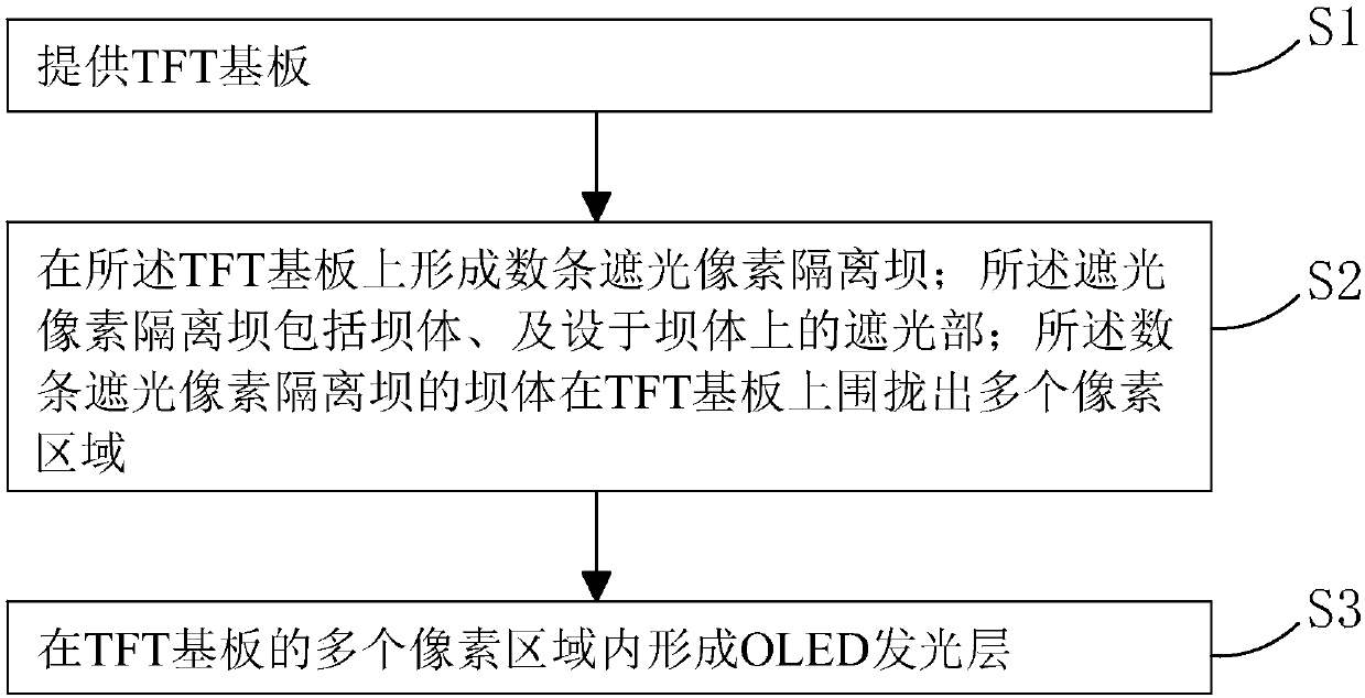
[0037] In order to further illustrate the technical means adopted by the present invention and its effects, the following describes in detail in conjunction with preferred embodiments of the present invention and accompanying drawings.

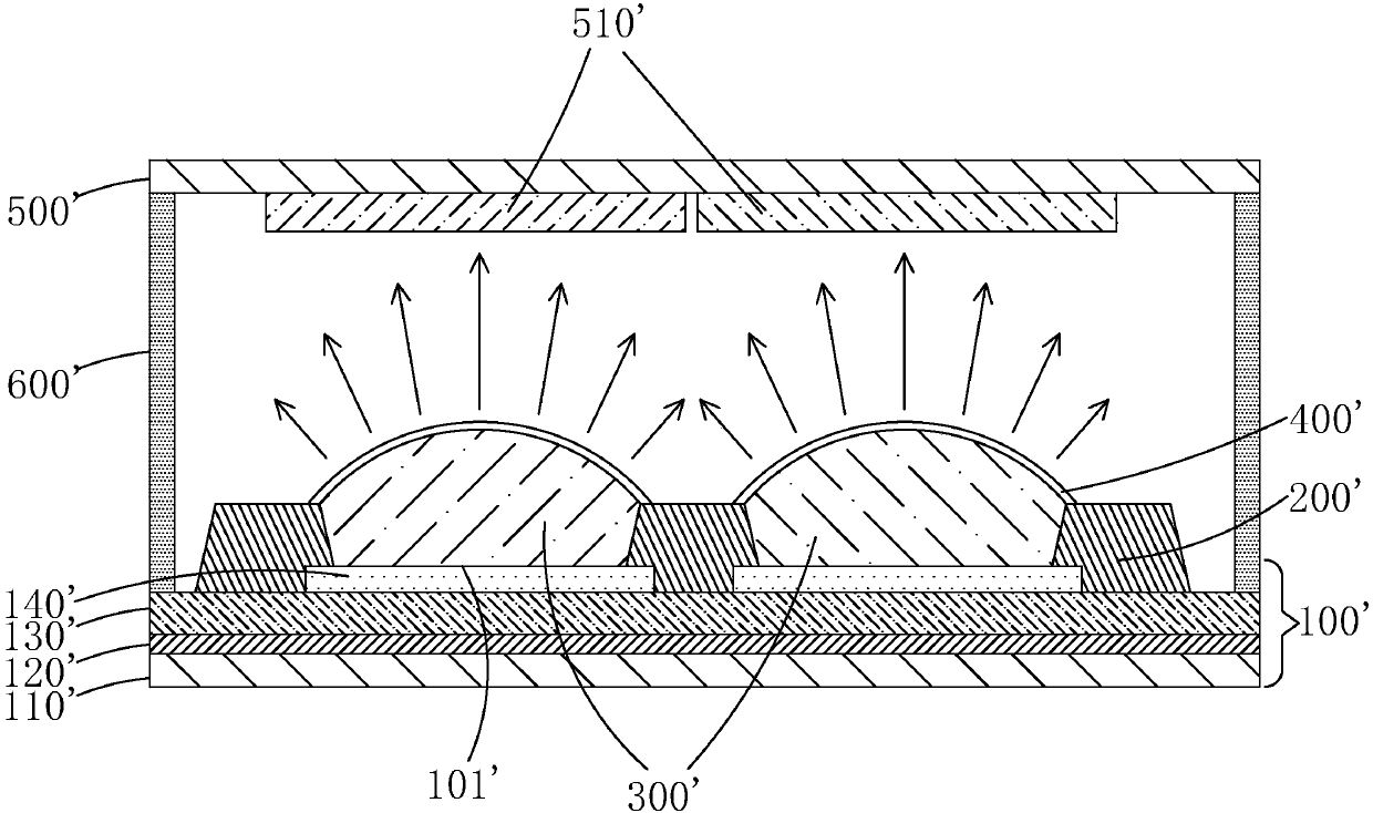
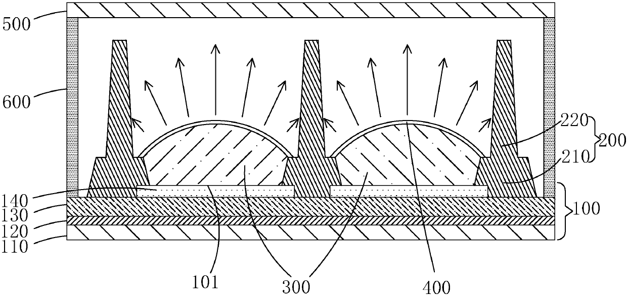
[0038] see figure 2 , the present invention provides an OLED display, comprising: a TFT substrate 100, several light-shielding pixel isolation dams 200 arranged on the TFT substrate 100, a plurality of OLED light-emitting layers 300 arranged on the TFT substrate 100, respectively arranged on multiple A plurality of cathodes 400 on each OLED light-emitting layer 300, an encapsulation cover 500 located above the light-shielding pixel isolation dam 200 and the cathode 400, and an encapsulation cover 500 and the TFT substrate 100 between the encapsulation cover 500 and the TFT substrate 100 Connected frame glue 600;

[0039] It should be noted that the light-shielding pixel isolation dam 200 includes a dam body 210 and a light-shielding portion ...


PUM


Abstract

The invention provides an OLED display device and a manufacturing method thereof. According to the OLED display device, a plurality of shading pixel isolation dams are arranged on a TFT substrate. Theshading pixel isolation dams include dam bodies and shading parts arranged on the dam bodies; a plurality of pixel regions are encircled by the dam bodies of the plurality of shading pixel isolationdams on the TFF substrate; and a plurality of OLED layers are arranged in the plurality of pixel regions. With the shading pixel isolation dams having shading parts, a problem of light leakage causedby inclined incidence of light in adjacent pixel regions during light emitting of the OLED layers is solved, so that the display effect of the OLED device is improved effectively.

Description

technical field [0001] The invention relates to the field of display technology, in particular to an OLED display and a manufacturing method thereof. Background technique [0002] Organic Light Emitting Display (OLED) has self-illumination, low driving voltage, high luminous efficiency, short response time, high definition and contrast, nearly 180° viewing angle, wide operating temperature range, and can realize flexible display and With many advantages such as large-area full-color display, it is recognized by the industry as a display device with the most potential for development. [0003] According to the driving method, OLED can be divided into two categories: passive matrix OLED (Passive Matrix OLED, PMOLED) and active matrix OLED (Active Matrix OLED, AMOLED), namely direct addressing and thin film transistor (TFT) matrix addressing. kind. Among them, AMOLED has pixels arranged in an array, belongs to the active display type, has high luminous efficiency, and is usua...

Claims


Application Information

Patent Timeline
Patent Type & Authority Applications(China)
IPC IPC(8): H01L27/32H01L51/52H01L21/77
CPCH10K59/122H10K59/1201H10K59/8791
Inventor 范英春任章淳张晓星
Owner SHENZHEN CHINA STAR OPTOELECTRONICS SEMICON DISPLAY TECH CO LTD
Why Eureka
Try Eureka