Eureka AIR delivers breakthrough ideas for toughest innovation challenges, trusted by R&D personnel around the world.

Polishing pad conditioning method and chemical mechanical polishing method including same

A chemical-mechanical and polishing pad technology, used in grinding/polishing equipment, parts of grinding machine tools, abrasive surface conditioning devices, etc., to solve problems such as over-polishing of the edge of the polishing pad, decreased wafer flatness, and increased surface defects. , to achieve the effect of reducing thickness consumption, reducing the number of defects on the wafer surface, and prolonging the service life

Active Publication Date: 2019-09-27
BEIJING SEMICORE PRECISION MICROELECTRONICS EQUIP CO LTD
View PDF6 Cites 0 Cited by
  • Summary
  • Abstract
  • Description
  • Claims
  • Application Information

AI Technical Summary

Problems solved by technology

[0006] The first object of the present invention is to provide a polishing pad dressing method to alleviate the problems that the edge of the polishing pad is easily over-polished by using the existing dressing method, which easily leads to a decrease in wafer flatness and an increase in surface defects

Method used


Image

  • Polishing pad conditioning method and chemical mechanical polishing method including same
  • Polishing pad conditioning method and chemical mechanical polishing method including same
  • Polishing pad conditioning method and chemical mechanical polishing method including same

Examples


Embodiment 1

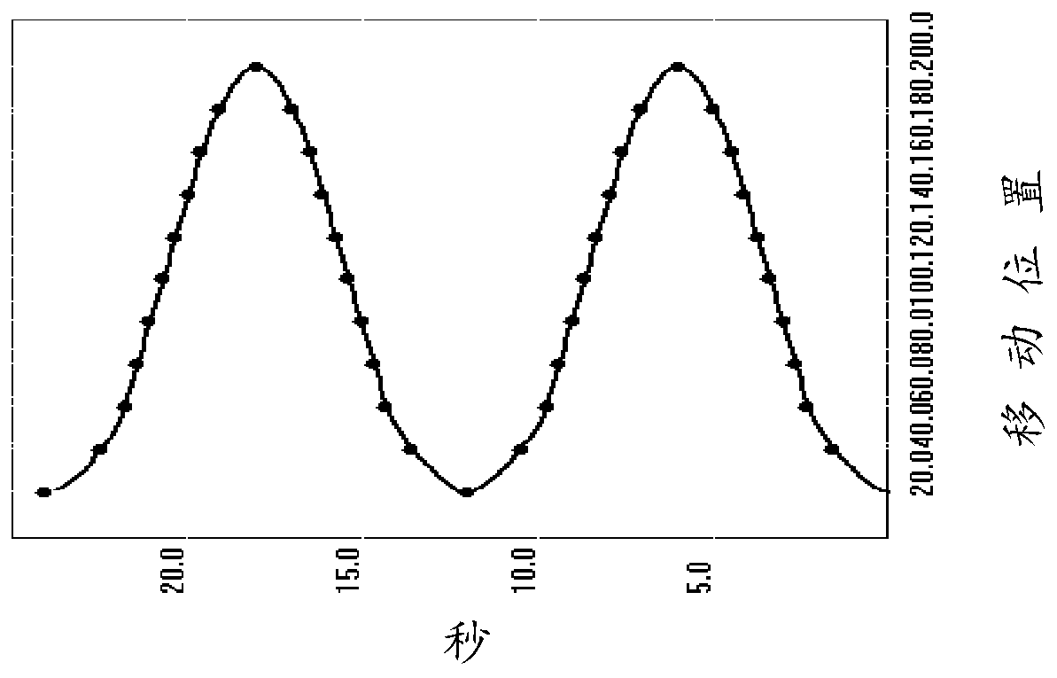
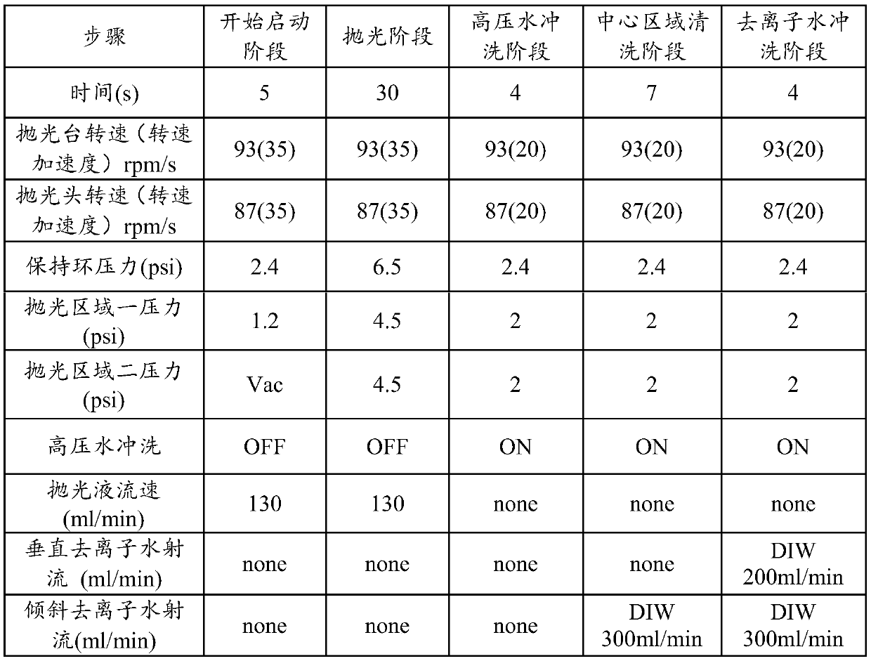
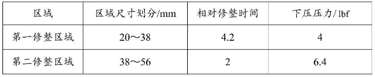
[0057] This embodiment is a chemical mechanical polishing method, wherein the polishing process and process parameters are listed in Table 1, and the trimming process parameters are listed in Table 2. The radius dimension of the polishing pad in this example is 254 mm and the size of the dresser is 108 mm.

[0058] Table 1 Polishing process and process parameters

[0059]

[0060] Table 2 trimming process parameters

[0061]

[0062]

[0063] Note, in the division of the area size in Table 2, the starting point 20mm is the edge of the polishing pad. 20mm. The move roadmap of the trimmer is as follows figure 1 shown.


PUM


Abstract

The invention provides a polishing pad dressing method, and a chemical mechanical polishing method comprising the polishing pad dressing method, and relates to the field of chemical mechanical polishing. The polishing pad dressing method comprises the steps that a dresser reciprocates between the edge and center of a polishing pad for dressing the polishing pad in the radial direction of the polishing pad; the polishing pad is divided into different dressing areas from the edge to the center of the dressing pad in sequence, and the relative dressing time and pressing pressure of the dresser indifferent dressing areas are different, so that the problems of excessive polishing of the polishing pad surface, reduction of wafer flatness, and increase of surface defects, caused by an existing dressing method easily, are solved; and the purposes of prolonging the service life of the polishing pad and reducing the wafer surface defects are achieved.

Description

technical field [0001] The invention relates to the technical field of chemical mechanical polishing of wafers, in particular to a polishing pad dressing method and a chemical mechanical polishing method comprising the same. Background technique [0002] With the reduction of the feature size of semiconductor devices, if there are excessive fluctuations on the surface of the wafer, it will become more and more difficult to control the line width in a series of subsequent processes. Therefore, in the semiconductor process flow, chemical mechanical polishing (CMP for short) is a very important process, and is sometimes called chemical mechanical planarization (CMP for short). The so-called chemical mechanical polishing is a process that uses chemical and mechanical combined action to remove excess material from semiconductor silicon wafers and obtain a flat surface. [0003] Chemical mechanical planarization is a key process to achieve global planarization of various material...

Claims


Application Information

Patent Timeline
Patent Type & Authority Patents(China)
IPC IPC(8): B24B53/00
Inventor 张康尹影李婷岳爽
Owner BEIJING SEMICORE PRECISION MICROELECTRONICS EQUIP CO LTD
Why Eureka
Eureka Blog
Learn More