A clamping circuit and a y-source inverter capable of increasing the boost ratio and suppressing DC bus voltage spikes
A technology of clamping circuit and source inverter, applied in the direction of converting AC power input to DC power output, electrical components, output power conversion devices, etc., can solve the problems of low circuit utilization efficiency and limited circuit power level, etc. Achieve high utilization rate, reduce impact, and increase boost ratio
- Summary
- Abstract
- Description
- Claims
- Application Information
AI Technical Summary
Problems solved by technology
Method used
Image
Examples
specific Embodiment approach 1
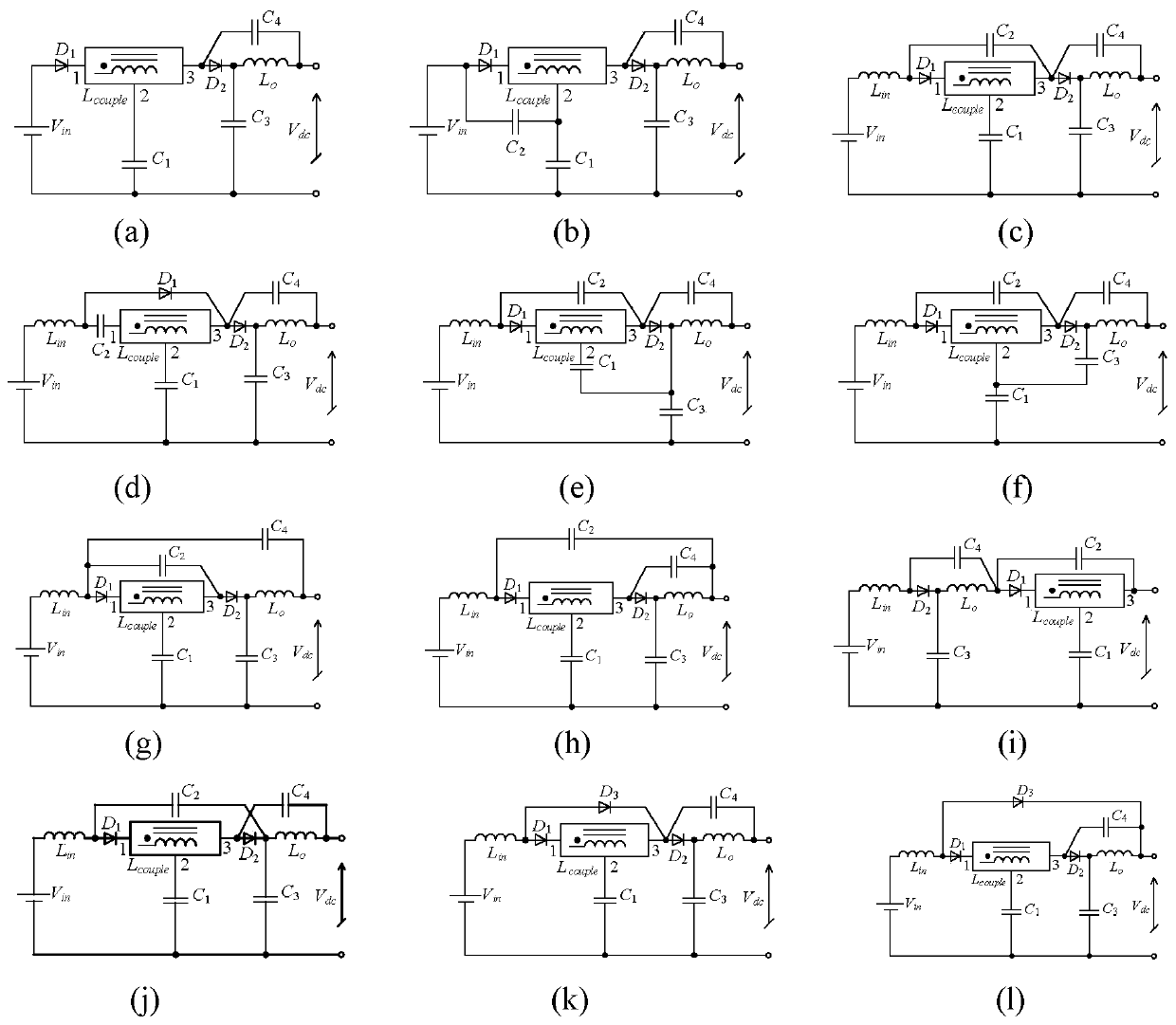
[0030] Specific embodiment one: reference figure 1 with figure 2 Detailed description of this embodiment, a clamp circuit described in this embodiment includes a capacitor C 3 , Capacitance C 4 , Diode D 2 And inductance L 0 ;
[0031] Diode D 2 The cathode is also connected to capacitor C 3 And inductance L 0 One end, capacitance C 4 Connect diode D to both ends of 2 Anode and inductance L 0 On the other end,
[0032] Diode D 2 Anode and capacitance C 3 The other end is used as the voltage input port of the clamp circuit, diode D 2 The anode is the positive input terminal, the capacitor C 3 The other end of is the reverse input end,
[0033] Inductance L 0 And capacitor C 3 The other end is used as the voltage output port of the clamp circuit, the inductor L 0 The other end is the positive output end, the capacitor C 3 The other end is the reverse output end.
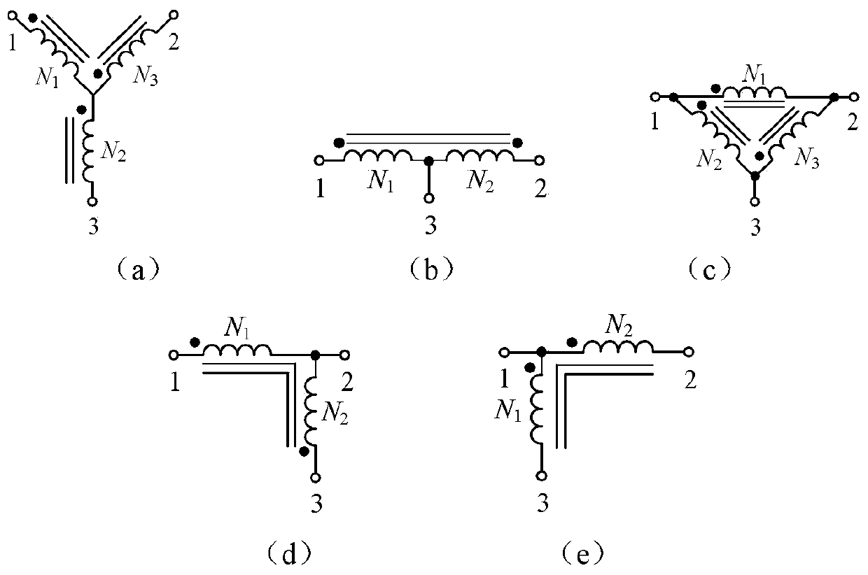
[0034] figure 1 L in coupled Indicates the coupled inductor in the inverter, the specific structure of the coupled inductor...
specific Embodiment approach 2
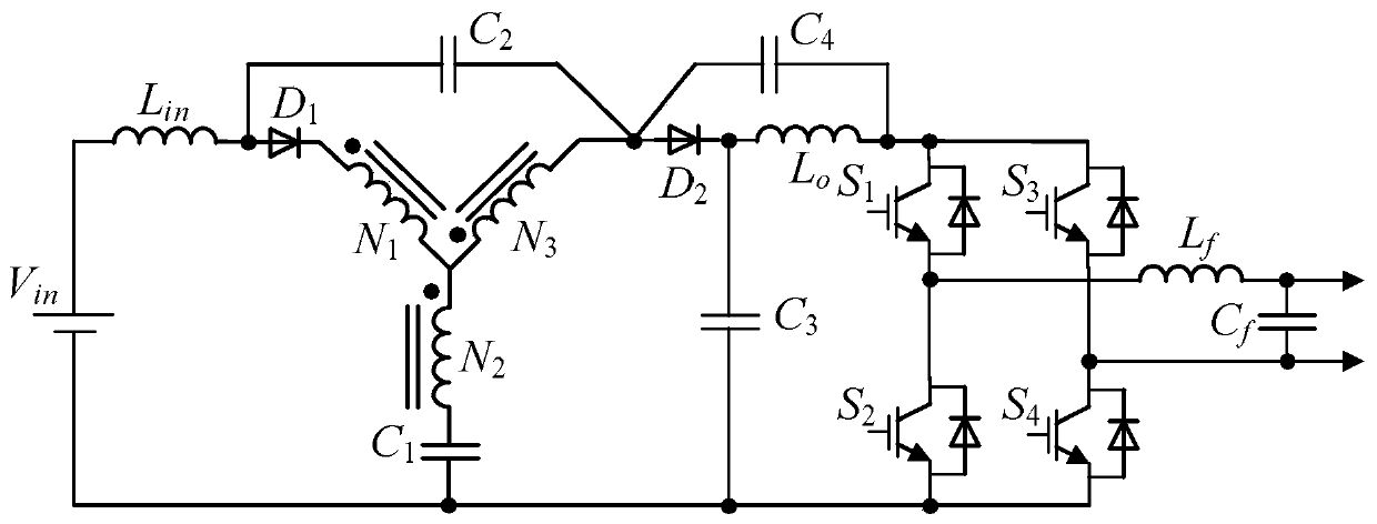
[0043] Specific embodiment two: reference Figure 3 to Figure 5 Detailed description of this embodiment, this embodiment is a Y-source inverter containing the clamping circuit described in the first embodiment, including a Y-source network circuit, a clamping circuit, and an inverter bridge circuit. The voltage output of the Y-source network circuit The port is connected to the voltage input port of the clamp circuit, and the voltage output port of the clamp circuit is connected to the voltage input port of the inverter bridge circuit. The inverter bridge circuit is used to supply power to the load or the power grid.
[0044] In this embodiment, the capacitance C 3 , Capacitance C 4 And diode D 2 It is used to clamp the voltage on the DC bus so that no voltage spikes will be generated on the DC bus.
specific Embodiment approach 3
[0045] Specific embodiment three: This embodiment is a further description of the Y-source inverter described in specific embodiment two. In this embodiment, the inverter bridge circuit is equivalent to a switch, and the Y-source inverter includes a through mode In the non-direct mode, the equivalent switch is closed in the direct mode, and the equivalent switch is open in the non-direct mode.
[0046] The Y-source inverter is divided into direct mode and non-direct mode when it is working. Among them, the direct mode and non-direct mode both include the linear region. In the linear region, the current on the leakage inductance will slowly change linearly, so there will be no large voltage spikes across the leakage inductance. The equivalent circuits in the two modes are as Figure 5 Shown. The AC output is equivalent to a current source, and the inverter bridge is equivalent to the switch tube SW. In the through mode, the equivalent switch SW is closed; and in the non-through ...
PUM
 Abstract
Description
Claims
Application Information


