Etching solution composition and method for manufacturing array substrate for display device

A composition and etching solution technology, applied in the directions of surface etching compositions, chemical instruments and methods, instruments, etc., can solve problems such as interface erosion when etching multilayer films, and achieve excellent etching profile and side etching variation characteristics. excellent effect

Active Publication Date: 2019-03-08
DONGWOO FINE CHEM CO LTD
View PDF1 Cites 0 Cited by
  • Summary
  • Abstract
  • Description
  • Claims
  • Application Information

AI Technical Summary

Problems solved by technology

However, the above-mentioned etchant has limitations in maintaining the taper angle that changes with time in the number of sheets processed when etching a thick-film metal layer, and there is a problem that the interface portion is corroded when etching a multilayer film.

Method used


Image

  • Etching solution composition and method for manufacturing array substrate for display device
  • Etching solution composition and method for manufacturing array substrate for display device
  • Etching solution composition and method for manufacturing array substrate for display device

Examples


Embodiment 1~9 and comparative example 1~8

[0094] Examples 1-9 and Comparative Examples 1-8. Preparation of Etching Solution Composition

[0095] 180 kg of etching liquid composition was manufactured according to the composition and content (weight%) described in the following Table 1.

[0096] [Table 1]

[0097]

[0098] Note) In the above table 1,

[0099] NHP: sodium dihydrogen phosphate

[0100] PPM: potassium dihydrogen phosphate

[0101] APM: Ammonium Phosphate

[0102] SS: sodium sulfate

[0103] PS: potassium sulfate

[0104] AS: Ammonium sulfate

[0105] TEG: Triethylene glycol (triethylene glycol)

[0106] Phosphite: sodium phosphite (sodium phosphite)

experiment example

[0107] Evaluation of Etching Properties of Etching Solution Composition

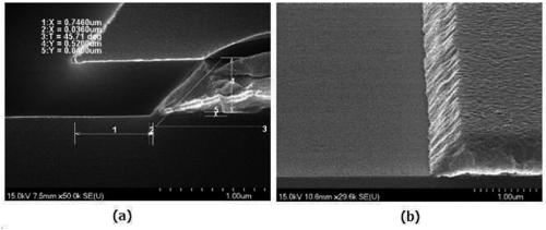
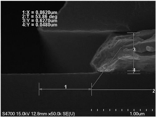
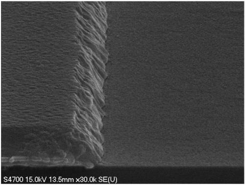
[0108] The etching process was implemented using the etching liquid composition of Examples 1-9 and Comparative Examples 1-8, respectively. The temperature of the etchant composition in the etching process was set to about 33° C. using a spray etching method experimental device (model name: ETCHER (TFT), SEMES). The etching time may vary depending on the etching temperature, but is usually performed at about 110 seconds. The profile cross section of the copper-based metal film etched in the above etching step was examined by SEM (Hitachi Corporation, model name S-4700), and the results are shown in Table 2 below.

[0109] The test piece (Cu / MoNb) used in the etching process used the following test piece: a molybdenum-niobium alloy film was deposited on a glass substrate (100mm×100mm), and a copper film was deposited on the above film, followed by a photolithography process. , forming a photoresist wit...

experiment example 1

[0110] Experimental example 1. Etching rate evaluation

[0111] Measure the end point detection (End Point Detection, EPD) with naked eyes, and obtain the etching rate (E / R, Etch Rate) at different times, and the etching rate is only evaluated by the vertical etching rate. If the thickness of the etched metal film is divided by the EPD, it can be calculated per second (time) (thickness) The etching rate was evaluated according to the following criteria, and the results are shown in Table 2.

[0112]

[0113] ○: good

[0114] Х: Poor (less than or more than )

[0115] Unetch: Unetchable


PUM


Abstract

The invention relates to an etchant composition, and a method for manufacturing an array substrate for a display device, and an array substrate and a display device. More specifically, the invention provides an etchant composition of a metal film uniformly etching the metal film, having the excellent etching speed and an excellent taper angle characteristic, and having an excellent etching profileof an interface unit in a case of etching of a multilayer when manufacturing an array substrate for a display device, a method for manufacturing an array substrate for a display device and an array for a display device. The etchant composition of the metal film is characterized by containing, with respect to the total weight of the composition, 5 to 25 wt% of hydrogen peroxide, 0.01 to 1 wt% of afluorine compound, 0.1 to 5 wt% of an azole compound, 0.1 to 5 wt% of a water-soluble compound having a nitrogen atom and a carboxyl group in one molecule is by weight, 0.001 to 5 wt% of a phosphatecontaining alkali metal or alkaline earth metal, 0.01 to 5 wt% of a polyol-type surfactant, 0.1 to 5 wt% of sulfate comprising alkali metal or alkaline earth metal, and the balance of water, the weight ratio of phosphate to sulfate being 1:3 to 1:20.

Description

technical field [0001] The invention relates to an etching solution composition and a method for manufacturing an array substrate for a display device. Background technique [0002] In a semiconductor device, the process of forming metal wiring on a substrate generally includes steps using the following processes: a metal film forming process using sputtering or the like; photoresist coating, exposure, and development using light in selective regions; A resist forming process; and an etching process, and includes cleaning processes before and after individual unit processes, and the like. Such an etching step refers to a step of leaving a metal film in a selective region using a photoresist as a mask, and generally, dry etching using plasma or the like or wet etching using an etchant composition is used. [0003] In such semiconductor devices, in recent years, the resistance of metal wiring has been mainly focused. This is because resistance is the main factor that induces...

Claims


Application Information

Patent Timeline
Patent Type & Authority Patents(China)
IPC IPC(8): C23F1/18C23F1/26H01L27/12
CPCC23F1/18C23F1/26H01L27/1214H01L27/1259C09K13/06C09K13/08C23F1/34C23F1/44G02F1/1362
Inventor 李恩远朴升煜田玹守梁承宰
Owner DONGWOO FINE CHEM CO LTD
Why Eureka
Try Eureka