Process for anisotropic etching of semiconductors

An anisotropic, semiconductor technology, used in semiconductor devices, semiconductor/solid-state device manufacturing, electrical components, etc., can solve problems such as low uniformity, and achieve the effect of improving the etching profile

Inactive Publication Date: 2015-03-25
3M INNOVATIVE PROPERTIES CO
View PDF11 Cites 0 Cited by
  • Summary
  • Abstract
  • Description
  • Claims
  • Application Information

AI Technical Summary

Problems solved by technology

Wet chemical etching can be isotropic and the process has low uniformity

Method used


Image

  • Process for anisotropic etching of semiconductors
  • Process for anisotropic etching of semiconductors
  • Process for anisotropic etching of semiconductors

Examples


example

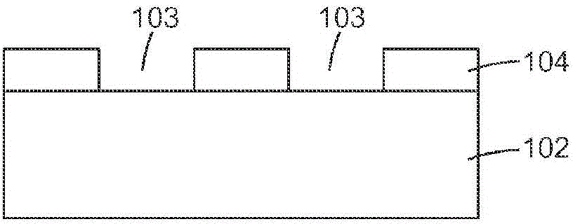
[0033] The II-VI semiconductor color conversion layer structure based on MgCdZnSe alloy was grown by molecular beam epitaxy on InP substrate. Structural details of color converting layers can be found, for example, in US Patent No. 7,402,831 (Miller et al.). The structure of the color conversion layer is schematically shown in figure 2 , the thickness and composition of its layers are shown in Table I below. figure 2 is a schematic diagram of the color conversion layer 200 , which includes a top window 202 , an absorber 204 , and a graded composition layer 206 that gradually changes from the composition of the top window 202 to the composition of the absorber 204 .

[0034] Table I

[0035] Composition of the color conversion layer structure

[0036] Floor

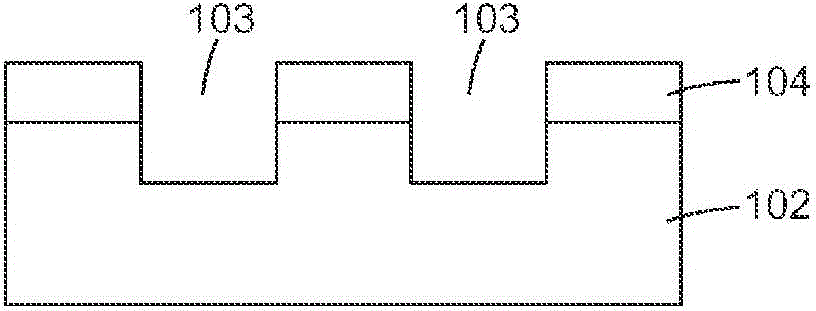
[0037] A raised photoresist pattern was generated on the II-VI semiconductor structures described above using a negative-tone photoresist (NR1-1000P from Futurrex, Franklin, NJ) and conventional contact...

example 1

[0040] Example 1 - Combined Ar etch and CHF 3 passivation

[0041] A sample of Comparative Example 1, also covered by a photoresist mask, was etched as follows:

[0042] a) Under the same conditions listed in Table I, the sample was etched by Ar sputtering for 30 seconds for the first time.

[0043] b) Turn off the plasma and argon supply, let trifluoromethane (CHF 3 ) into the process chamber at a rate of 40 sccm for 30 seconds.

[0044] c) Restore the plasma and use 5-40sccm CHF 3 , 20-200 watts of Rf power, 700-2000 watts of inductively coupled plasma power, a pressure of 4-30 mTorr and an etching time of 5 seconds for plasma polymerization of trifluoromethane.

[0045] d) Shut off the trifluoromethane supply and let Ar gas flow into the chamber at 40 sccm for 30 seconds.

[0046] e) Repeat steps a) to d) for a total of 8 times.

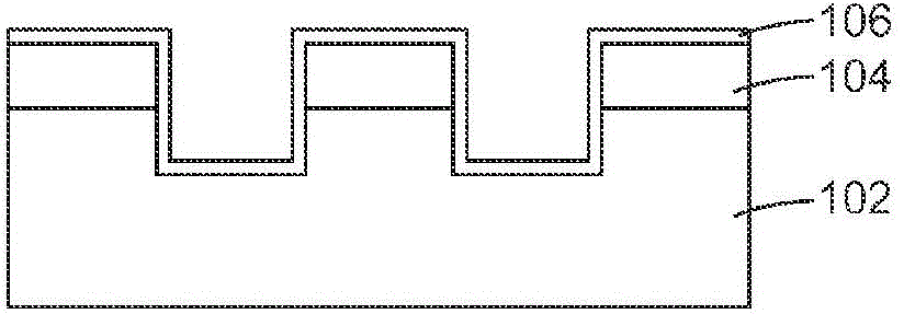
[0047] Figure 4 are scanning electron micrographs of CdMgZnSe crystals using processes a) to e). It can be observed that an etch p...

example 2

[0049] A sample from Comparative Example 1 overlaid by a photoresist mask made with NR9-300PY negative photoresist (from Futurrex, Franklin, NJ) was etched using the procedure of Example 1, except that Ar etch for 60 seconds and steps a) to d) were repeated 6 times. Figure 5 is a scanning electron micrograph of the resulting structure and shows deep etching of II-VI material with wall angles of almost 90 degrees. It is calculated that the etching rate of the semiconductor material is 341 nm / min, while the etching rate of the photoresist material is 126 nm / min.


PUM


Abstract

A method is provided for anisotropically etching semiconductor materials such as II-VI and III-V semiconductors. The method involves repeated cycles of plasma sputter etching of semiconductor material with a non-reactive gas through an etch mask, followed by passivation of the side walls by plasma polymerization using a polymer former. Using this procedure small pixels in down-converted light-emitting diode devices can be fabricated.

Description

technical field [0001] The present disclosure broadly relates to a process for anisotropic etching of semiconductors. Background technique [0002] The rapid development of optoelectronics has created a need for methods to fabricate nanoscale patterns on semiconductor surfaces. Typically, these patterns are etched into the semiconductor substrate by a variety of techniques. For example, wet chemical etching has been used to etch various semiconductors. Typically, in the case of II-VI semiconductors such as ZnSe, wet chemical etching uses bromine-based chemicals. Wet chemical etching is carried out by oxidation of the semiconductor component followed by chemical dissolution of the oxide in a suitable solvent. Wet chemical etching can be isotropic and the process has low uniformity. The production industry in the optoelectronics industry requires a more controlled etching process than can be achieved using wet etching. [0003] Due to the many disadvantages of wet chemica...

Claims


Application Information

Patent Timeline
Patent Type & Authority Patents(China)
IPC IPC(8): H01L21/3065
CPCH01L33/20H01L21/465H01L21/3065
Inventor 特里·L·史密斯张俊颖
Owner 3M INNOVATIVE PROPERTIES CO
Why Eureka
Try Eureka