The etching composition for etching conductive multi -layer membrane and the etching method using it

A composition and etchant technology, applied in the directions of surface etching compositions, chemical instruments and methods, circuits, etc., can solve problems such as rising demand for metallization layers, and achieve the effects of simplifying production costs and time, and reducing processes

Inactive Publication Date: 2016-01-13
PLANSEE SE
View PDF9 Cites 0 Cited by
  • Summary
  • Abstract
  • Description
  • Claims
  • Application Information

AI Technical Summary

Problems solved by technology

However, for larger size touch sensors, the need for lower resistivity metallization layers rises, and as a result, multilayer films of Cu / Mo or Cu / Mo alloys must be used

Method used


Image

  • The etching composition for etching conductive multi -layer membrane and the etching method using it
  • The etching composition for etching conductive multi -layer membrane and the etching method using it
  • The etching composition for etching conductive multi -layer membrane and the etching method using it

Examples


experiment Embodiment 1

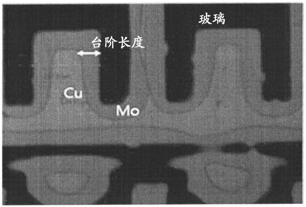
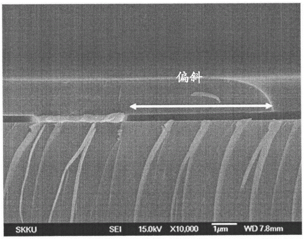
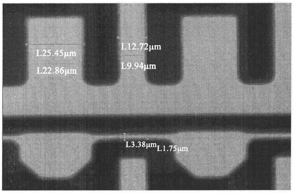
[0058] A Cu / Mo bilayer film was deposited on a substrate and a photoresist (PR) was formed thereon to fabricate a sample. The etchant of Example 1 and Comparative Example 1 were each placed in a spray type etching system (FNSTech.) and heated to 40°C. When the temperature reaches 40±0.1°C, etchant is used to etch the Cu / Mo bilayer film. Etch times were over 50% etch with endpoint detection (EPD). After the etching was completed, the substrate was taken out of the etching system, washed with deionized water, and dried using a hot air dryer. Use a photoresist stripper to remove the photoresist. Critical dimension (CD) skew (etch loss), step length as a width difference between copper and molybdenum layers, and etch residue of etched structures were evaluated using scanning electron microscopy (SEM, TESCAN).

Embodiment 1

[0061]Specifically, KR2006-0082270A discloses an etchant composition for etching metal electrodes to form thin film transistors of flat panel displays. In addition to phosphoric acid, nitric acid, acetic acid, and water, which are components of a typical etchant for etching aluminum, the etchant composition contains an etch rate control agent to form a desired pattern. According to Example 1 of this prior art, the etchant has the following composition:

[0062] h 3 PO 4 (55% by weight)+HNO 3 (8% by weight)+CH3COOH (10% by weight)+(NH 4 ) 2 HPO 4 (2wt%)+CH 3 COONH 4 (2% by weight)+H 2 O (surplus).

[0063] The etching properties of the etchant were tested. The results are shown in Figure 1a and 1b middle.

[0064] specifically, Figure 1a Shows detailed results obtained when applying the etchant of Comparative Example 1 to a Cu / Mo bilayer film as proposed in the prior art (KR2006-0082270A) embodiment comprising phosphoric acid, nitric acid, and at least one additi...

Embodiment 2

[0073] h 3 PO 4 (70% by weight)+HNO 3 (2wt%)+CH 3 COOH (15% by weight) + imidazole (C 3 h 4 N 2 , 0.1 to 0.3% by weight) + distilled water (balance).


PUM


Abstract

PROBLEM TO BE SOLVED: To provide an etchant composition which can efficiently, excellently, simultaneously and collectively etch a multiple film including a copper layer comprises one or more layers of copper or copper alloy such as a Cu / Mo laminated metal film, a Cu / Mo alloy laminated metal film and a Cu alloy / Mo alloy laminated metal film, and a molybdenum layer comprises one or more layers of molybdenum or molybdenum alloy, and to provide a etching method for the multiple film using the same.SOLUTION: The etchant composition contains 50-80 wt.% of phosphoric acid, 0.5-10 wt.% of nitric acid, 5-30 wt.% of acetic acid, 0.01-5 wt.% of imidazole with respect to the total weight, and the balance water. The imidazole as an additive functions as a copper / molybdenum galvanic reaction controller.

Description

technical field [0001] The present invention relates to etchant compositions for patterning conductive layers used in thin film transistors (TFTs) of flat panel displays or touch sensor panels. More specifically, the present invention relates to methods for etching conductive multilayer films comprising at least one layer of copper (Cu) or copper alloy (Cu alloy) and at least one layer of molybdenum (Mo) or molybdenum alloy (Mo alloy), especially for An etchant composition for etching a Cu / Mo bilayer film in one pass. The present invention also relates to a method of etching a conductive multilayer film using the etchant composition. Background technique [0002] A double-layer film consisting of a Cu layer and a molybdenum (Mo) or titanium (Ti) layer below the Cu layer as a diffusion barrier is currently used instead of a copper (Cu) single layer as a low-resistance metal electrode for TFTs , such as gate electrodes or source / drain electrodes. Many etchants for such bila...

Claims


Application Information

Patent Timeline
Patent Type & Authority Patents(China)
IPC IPC(8): C23F1/18C23F1/26C23F1/02
CPCC09K13/04C23F1/02C23F1/18C23F1/26H01L21/308
Inventor 徐宗铉
Owner PLANSEE SE
Why Eureka
Try Eureka