Chip antenna and electronic equipment using the chip antenna

A chip antenna, patch antenna technology, applied in the direction of antenna, antenna array, antenna components, etc., can solve the problem that the signal cannot be radiated to a wider angle range, and achieve the effect of widening the signal radiation angle and improving the omnidirectionality.

Active Publication Date: 2021-01-26
SHENZHEN SHENGLU IOT COMM TECH CO LTD
View PDF4 Cites 0 Cited by
  • Summary
  • Abstract
  • Description
  • Claims
  • Application Information

AI Technical Summary

Problems solved by technology

[0005] In view of the above situation, the purpose of the present invention is mainly to solve the problem that the existing chip antenna cannot radiate signals to a wider range of angles during actual signal transmission

Method used


Image

  • Chip antenna and electronic equipment using the chip antenna
  • Chip antenna and electronic equipment using the chip antenna
  • Chip antenna and electronic equipment using the chip antenna

Examples


Embodiment 1

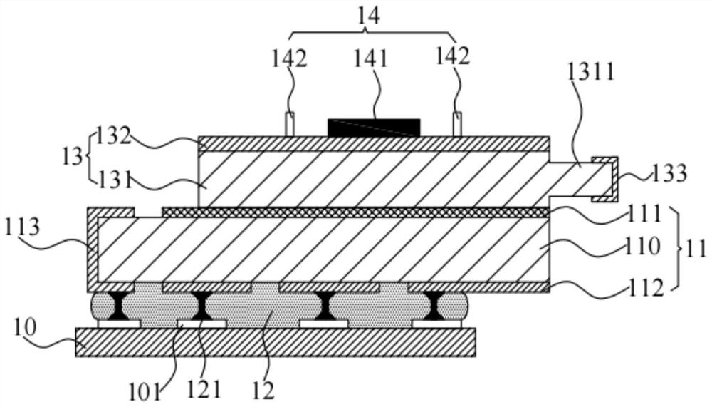
[0037]SeeFigure 1 to Figure 3 , A chip antenna includes a base chip 10, wherein a first patch antenna 11 and a second patch antenna 13 are provided above the base chip 10, and the upper surface of the first patch antenna 11 is The lower surfaces of the second patch antenna 13 are attached to each other.

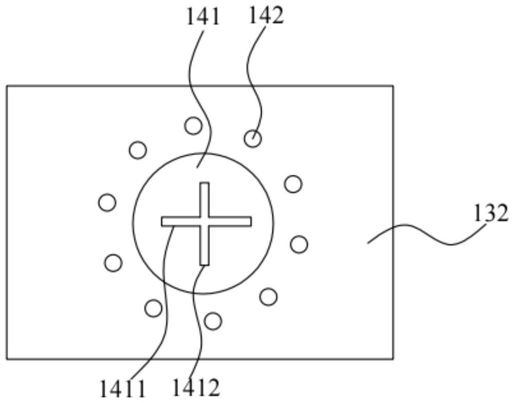
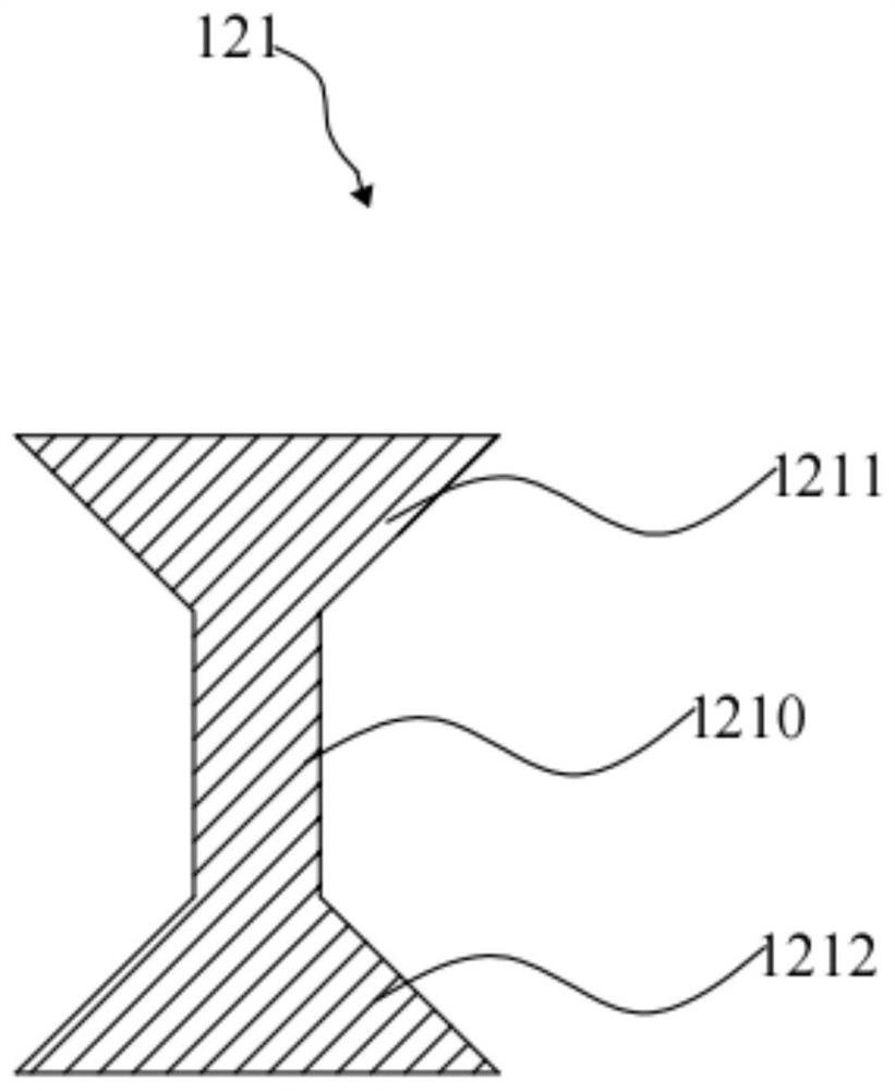
[0038]Wherein, the first patch antenna 11 includes a metal microstrip feed line 111, a first dielectric layer 110, and a first conductive layer 112 arranged in order from top to bottom. The second patch antenna 13 includes a metal radiation patch 132 and a second dielectric layer 131 arranged in order from top to bottom. In addition, an underfill layer 12 is also provided between the base chip 10 and the first patch antenna 11, and the base chip 10 and the first patch antenna 11 are electrically connected. A signal emitting component 14 is provided on the upper surface of the metal radiation patch 132. The signal emitting component 14 includes a signal radiating part 141 for emitting ...

Embodiment 2

[0045]SeeFigure 4 to Figure 6 , A chip antenna includes a base chip 10, wherein a first patch antenna 11 and a second patch antenna 13 are provided above the base chip 10, and the upper surface of the first patch antenna 11 is The lower surfaces of the second patch antenna 13 are attached to each other.

[0046]Wherein, the first patch antenna 11 includes a metal microstrip feed line 111, a first dielectric layer 110, and a first conductive layer 112 arranged in order from top to bottom. The second patch antenna 13 includes a metal radiation patch 132 and a second dielectric layer 131 arranged in order from top to bottom. In addition, an underfill layer 12 is also provided between the base chip 10 and the first patch antenna 11, and the base chip 10 and the first patch antenna 11 are electrically connected. A signal emitting component 14 is provided on the upper surface of the metal radiation patch 132, and the signal emitting component 14 includes a signal radiating part 141a for emit...

Embodiment 3

[0054]SeeFigure 7 to Figure 9 , A chip antenna includes a base chip 10, wherein a first patch antenna 11 and a second patch antenna 13 are provided above the base chip 10, and the upper surface of the first patch antenna 11 is The lower surfaces of the second patch antenna 13 are attached to each other.

[0055]Wherein, the first patch antenna 11 includes a metal microstrip feed line 111, a first dielectric layer 110, and a first conductive layer 112 arranged in order from top to bottom. The second patch antenna 13 includes a metal radiation patch 132 and a second dielectric layer 131 arranged in order from top to bottom. In addition, an underfill layer 12 is also provided between the base chip 10 and the first patch antenna 11, and the base chip 10 and the first patch antenna 11 are electrically connected. A signal emitting component 14 is provided on the upper surface of the metal radiation patch 132, and the signal emitting component 14 includes a signal radiating part 141a for emit...


PUM

PropertyMeasurementUnit
heightaaaaaaaaaa
heightaaaaaaaaaa

Abstract

A chip antenna comprises a substrate chip, a first patch antenna and a second patch antenna, wherein the first patch antenna and the second patch antenna are arranged above the substrate chip, an upper surface of the first patch antenna is attached onto a lower surface of the second patch antenna, the first patch antenna comprises a metal microstrip feeder, a first dielectric layer and a first conductive layer which are sequentially arranged from top to bottom, the second patch antenna comprises a metal radiation patch and a second dielectric layer which are sequentially arranged from top to bottom, a bottom filler layer is arranged between the substrate chip and the first patch antenna, the substrate chip and the first patch antenna are electrically connected, a signal emission assembly is arranged on an upper surface of the metal radiation patch and comprises a signal emission part and a plurality of micro vertical posts, the signal emission part is used for emitting a signal towardsa circumferential direction, and the plurality of micro vertical posts are uniformly arranged in a way that the signal emission part is encircled. With the chip antenna proposed by the invention, thesignal radiation angle is greatly expanded, and the signal emission omnidirectivity is improved.

Description

Technical field[0001]The present invention relates to the field of chip technology, in particular to a chip antenna and electronic equipment using the chip antenna.Background technique[0002]In recent years, with the rapid development of wireless communication systems, the requirements for antennas have become higher and higher. Traditional whip antennas and helical antennas have been gradually replaced by built-in small antennas because they cannot meet actual needs.[0003]Currently, dielectric chip antennas are being produced and used on a large scale due to their small size, light weight, and stable electrical characteristics. Moreover, the production cost is relatively low, and it has a good economic advantage in industrial production, so it is produced and applied on a large scale.[0004]However, when the existing dielectric chip antennas actually transmit signals, their omnidirectional performance is not satisfactory. That is, when the signal is transmitted, the signal cannot be ...

Claims


Application Information

Patent Timeline
Patent Type & Authority Patents(China)
IPC IPC(8): H01Q1/22H01Q1/36H01Q1/38H01Q21/00
CPCH01Q1/2283H01Q1/36H01Q1/38H01Q21/00
Inventor 杜光东
Owner SHENZHEN SHENGLU IOT COMM TECH CO LTD
Why Eureka
Try Eureka