A chip angle correction device for LED packaging

A technology of LED packaging and angle correction, which is applied to semiconductor devices, electrical components, circuits, etc., can solve the problems of reducing error rate, speeding up chip correction speed, and speeding up chip processing process, etc.

Active Publication Date: 2019-08-02
安徽三优光电科技有限公司
View PDF2 Cites 1 Cited by
  • Summary
  • Abstract
  • Description
  • Claims
  • Application Information

AI Technical Summary

Problems solved by technology

[0005] Aiming at the deficiencies in the prior art, the purpose of the present invention is to provide a chip angle correction device for LED packaging to solve the problem of correcting the position of the chip during soldering when using the prior art. In order to ensure the accuracy of welding and realize the rapid correction of the chip, a set of high-speed and high-precision correction mechanism is needed to speed up the chip correction speed and the chip processing process, and at the same time Problems that can reduce the error rate

Method used


Image

  • A chip angle correction device for LED packaging
  • A chip angle correction device for LED packaging
  • A chip angle correction device for LED packaging

Examples


Embodiment Construction

[0024] In order to make the technical means, creative features, goals and effects achieved by the present invention easy to understand, the present invention will be further described below in conjunction with specific embodiments.

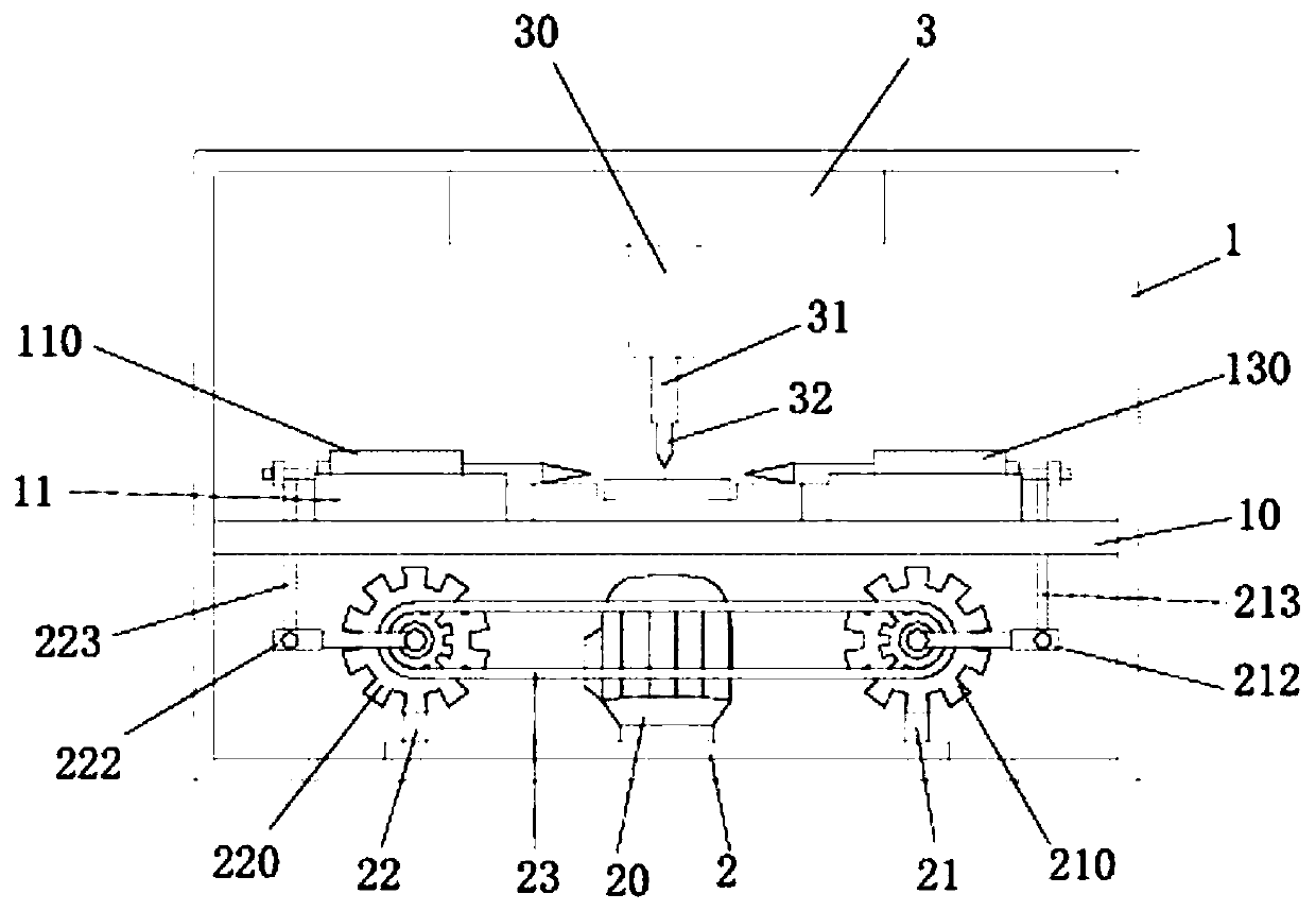
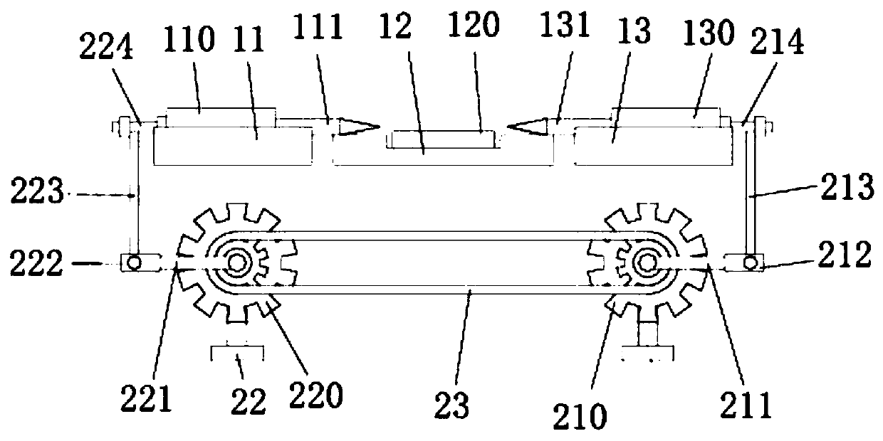
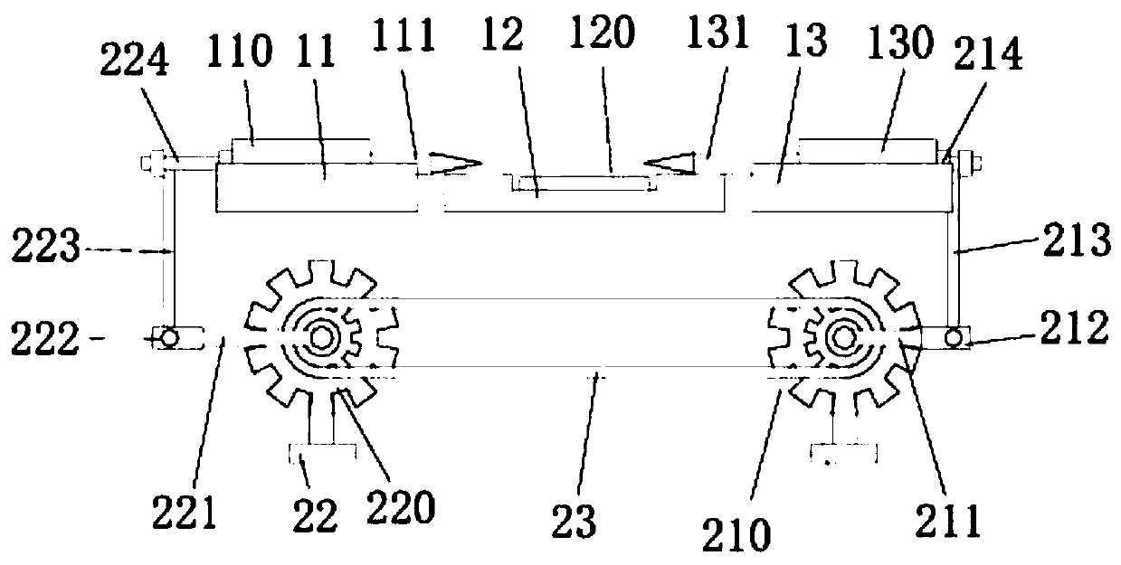
[0025] see Figure 1-Figure 7 , the present invention provides a technical scheme of a chip angle correction device for LED packaging: its structure includes a straightening machine main body 1, a transmission base 2, and a welding base 3, and the straightening machine main body 1 is riveted to an internal transmission platform 10 by bolts On the outer surface, the transmission base 2 is connected to the inner bottom surface of the straightening machine main body 1 by bolt riveting, and the welding base 3 is connected to the inner upper wall of the straightening machine main body 1 by bolt riveting, and the straightening machine main body 1 is set There is an internal transmission table 10, a first straightening control base 11, a workpiece fixing...


PUM


Abstract

The invention discloses a chip angle correction device for LED packaging, and the structure of the device comprises a straightening machine main body, a drive stand, and a welding base. The drive stand is provided with a drive motor, a first transmission gear support, a second transmission gear support, and a conveying belt. The first transmission gear support is provided with a first transmissiongear, a first gear push rod, a first gear push rod fixing shaft, a first support rod, and a first rectifying support rod. The welding base is provided with a welding air pressure main rod, a weldingair pressure support rod, and a welding head, thereby achieving the fixing of a chip through a workpiece fixing table when the device is in use, reducing the movement range, and improving the weldingprecision. Meanwhile, the device can achieve the ordered rectification through a rectifying device, enables the chip rectification to be quick through the bidirectional repeated quick rectification, speeds up the rectification speed of the chip, increases the speed of chip processing, reduces the error rate of chip welding, and avoids the material waste.

Description

technical field [0001] The invention relates to a chip angle correction device for LED packaging, which belongs to the field of chip angle correction devices. Background technique [0002] In recent years, with the development of the LED industry, an industrial chain with high technical content and broad market prospects has been formed in the application of materials, chips, packaging and LED lighting. In particular, high-power, high-brightness LED modules have become an international semiconductor lighting industry And show the hot spots of competition in the field. [0003] The new generation of high-power LED module packaging technology and equipment manufacturing is the research focus of the world's leading LED companies and research institutions. The barriers in the core technology of high-power and high-brightness LED industry development are gradually forming. LED packaging technology It is a precision assembly and manufacturing technology that bonds, fixes and seal...

Claims


Application Information

Patent Timeline
Patent Type & Authority Patents(China)
IPC IPC(8): H01L33/48H01L33/62
CPCH01L33/48H01L33/62H01L2933/0033H01L2933/0066
Inventor 王孝裕
Owner 安徽三优光电科技有限公司
Why Eureka
Try Eureka