Hardware framework for carrying out reasoning acceleration by aiming at convolution neural network, and working method thereof
A neuron network and hardware architecture technology, applied in the field of integrated circuit processor hierarchy design, can solve the problems of idle computing units, high power consumption, and inability to apply embedded devices
- Summary
- Abstract
- Description
- Claims
- Application Information
AI Technical Summary
Problems solved by technology
Method used
Image
Examples
Embodiment 1
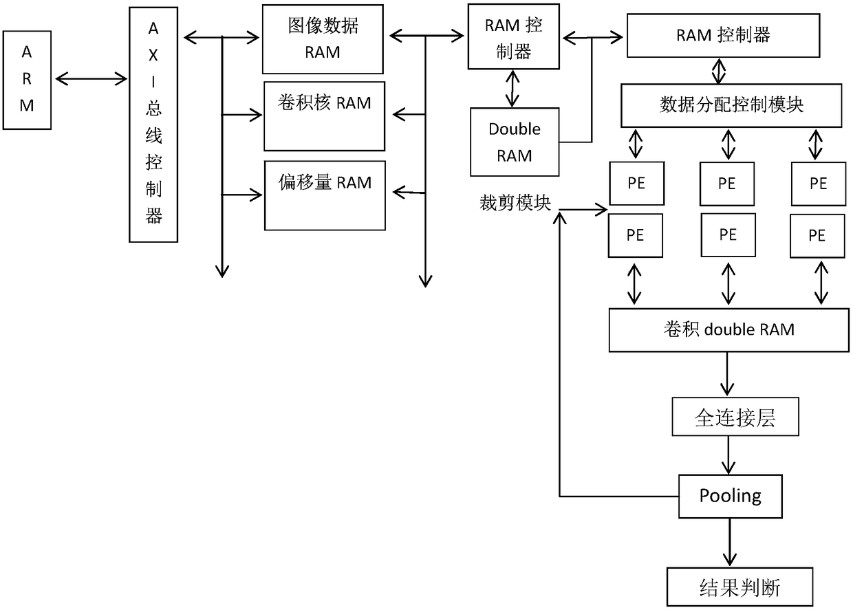
[0066] A hardware architecture for inference acceleration for convolutional neural networks, such as figure 1 As shown, including a preprocessing unit, a hardware acceleration unit, and a storage unit;
[0067] The preprocessing unit is used to preprocess the input original image frame;
[0068] The hardware acceleration unit is used to read in the filled image frame to be convoluted, the convolution kernel coefficient, and the offset parameter for convolution. After the convolution is completed, the calculation of the fully connected layer is performed. After the calculation of the fully connected layer is completed, the output calculation Feature judgment result, calculating the feature judgment result refers to judging the probability that the input picture conforms to each different result; that is, inferring and judging the input picture and then outputting the result, that is, judging the probability that the input picture conforms to each different result.
[0069] The...
Embodiment 2
[0071] According to a hardware architecture for reasoning acceleration of convolutional neuron networks described in Embodiment 1, the difference is that,
[0072] The preprocessing unit includes ARM, and the preprocessing unit is connected to the hardware acceleration unit through the AXI bus controller; the CPU (ARM) is the FPGA's own CPU, and supports the AXI bus structure, and the FPGA logic performs data interaction with the ARM through the AXI bus structure. The hardware acceleration unit includes several RAMs, RAM controllers, cropping modules, address control modules, data allocation control modules, and convolution array modules; all RAMs are composed of double buffers to improve efficiency. The RAM is a double buffer, which increases data sharing, reduces data read redundancy, and considers maximizing support for parallel PE computing.
[0073] ARM sequentially performs image supplementation on the input original image frame, converts floating-point data to fixed-poi...
Embodiment 3
[0076] The working method of the hardware architecture described in embodiment 2 includes:
[0077] (1) ARM preprocesses the input original image frame. The preprocessing includes sequentially performing image supplementation, converting floating-point data to fixed-point data, and configuring the logic register of FPGA; converting floating-point data to fixed-point data refers to converting floating-point data to fixed-point 8bits data. Configuring the logical registers of the FPGA refers to sending data such as weights and offsets to the logical registers using the AXI bus. After the configuration is completed, the input image can be used for inference. The connection relationship of the logic registers of the FPGA is fixed inside the FPGA, such as figure 1 shown;
[0078] (2) The AXI bus controller reads the filled image frame to be convoluted, the convolution kernel coefficient, and the offset parameter to several RAMs; including: the AXI bus controller judges the origin...
PUM
 Abstract
Description
Claims
Application Information


