Transformer and power supply device
A transformer and device technology, applied in the field of transformers and power supply devices, can solve the problems of manual completion of the shielding layer, a large amount of manpower and time, and difficulty in determining the optimal number of turns of the shielding layer, so as to shorten the verification cycle, reduce production costs, and simplify design. The effect of debugging
- Summary
- Abstract
- Description
- Claims
- Application Information
AI Technical Summary
Problems solved by technology
Method used
Image

Examples
Embodiment Construction
[0054] The technical solutions in the embodiments of the present application will be described below with reference to the drawings in the embodiments of the present application.
[0055] The embodiment of the present application provides a transformer, which can achieve the best shielding effect of transformer common-mode noise in a short period of time, shorten the transformer design cycle, and reduce research and development and production costs.
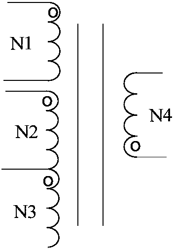
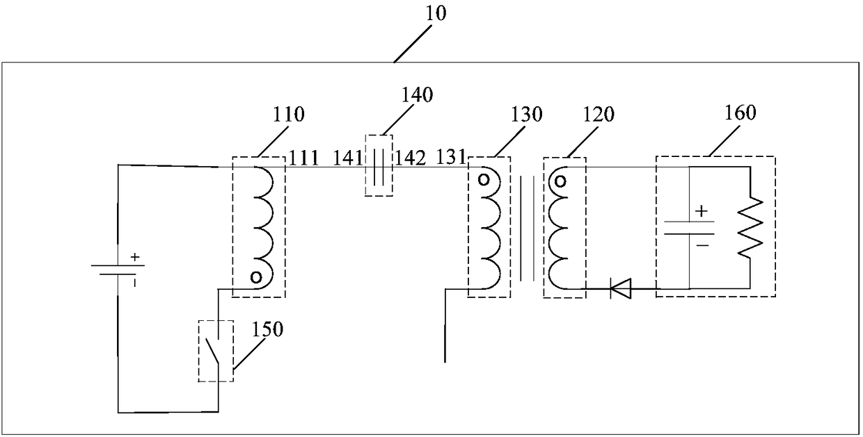
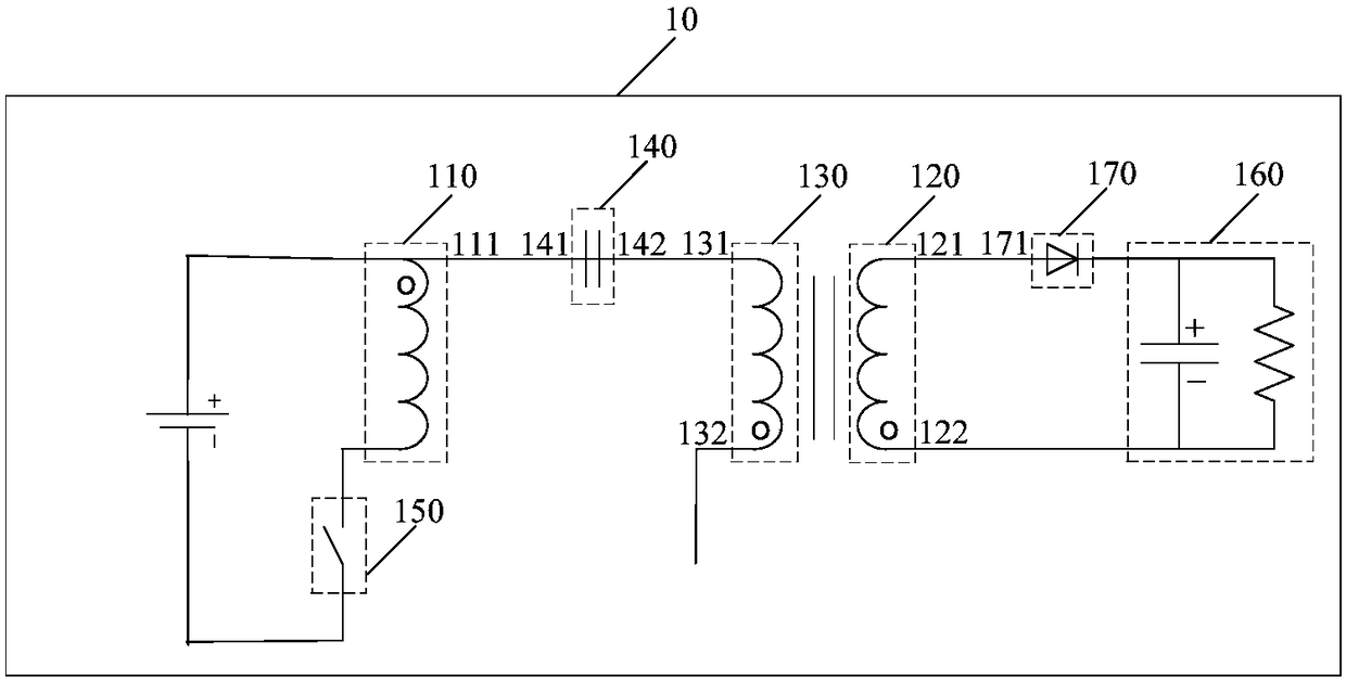
[0056] See figure 2 , figure 2 It is a structural schematic diagram of a transformer circuit provided in the embodiment of the present application, such as figure 2 As shown, the transformer circuit 10 may at least include:
[0057] Primary winding 110, secondary winding 120, shielding winding 130 and adjustable impedance device 140;
[0058] The first end 111 of the above-mentioned primary winding 110 is connected to the first end 141 of the above-mentioned adjustable impedance device 140, and the second end 142 of the abo...
PUM
 Abstract
Description
Claims
Application Information
 - R&D Engineer
- R&D Manager
- IP Professional
- Industry Leading Data Capabilities
- Powerful AI technology
- Patent DNA Extraction
Browse by: Latest US Patents, China's latest patents, Technical Efficacy Thesaurus, Application Domain, Technology Topic.
© 2024 PatSnap. All rights reserved.Legal|Privacy policy|Modern Slavery Act Transparency Statement|Sitemap