
Hall element and Hall element structure

A technology of Hall element and Hall voltage, applied in the field of Hall element structure and Hall element, can solve the problems that affect product design and production cycle, affect the normal operation of product design company, and cannot be corrected, and shorten the design verification cycle. , reduce the number of design modifications, and improve the effect of testability

Active Publication Date: 2017-06-09
SHANGHAI INTEGRATED CIRCUIT RES & DEV CENT +1
View PDF6 Cites 0 Cited by
  • Summary
  • Abstract
  • Description
  • Claims
  • Application Information

AI Technical Summary

Problems solved by technology

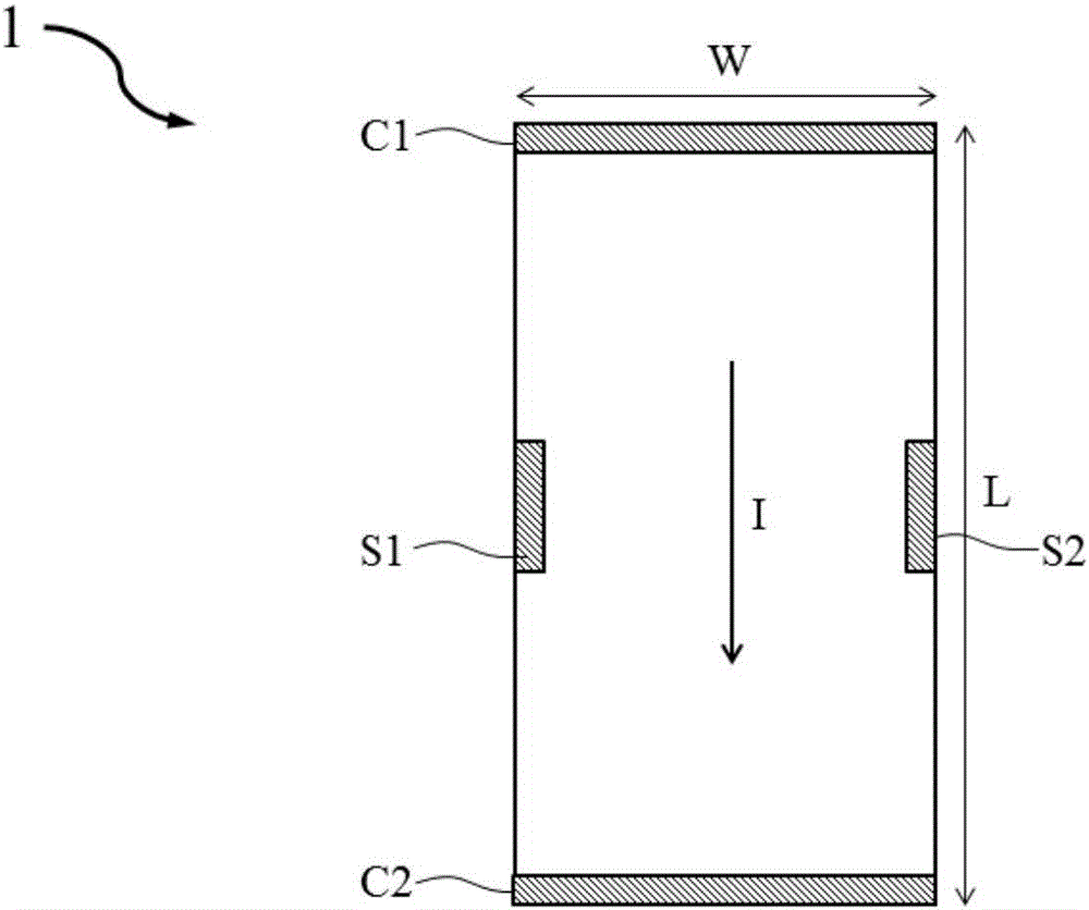
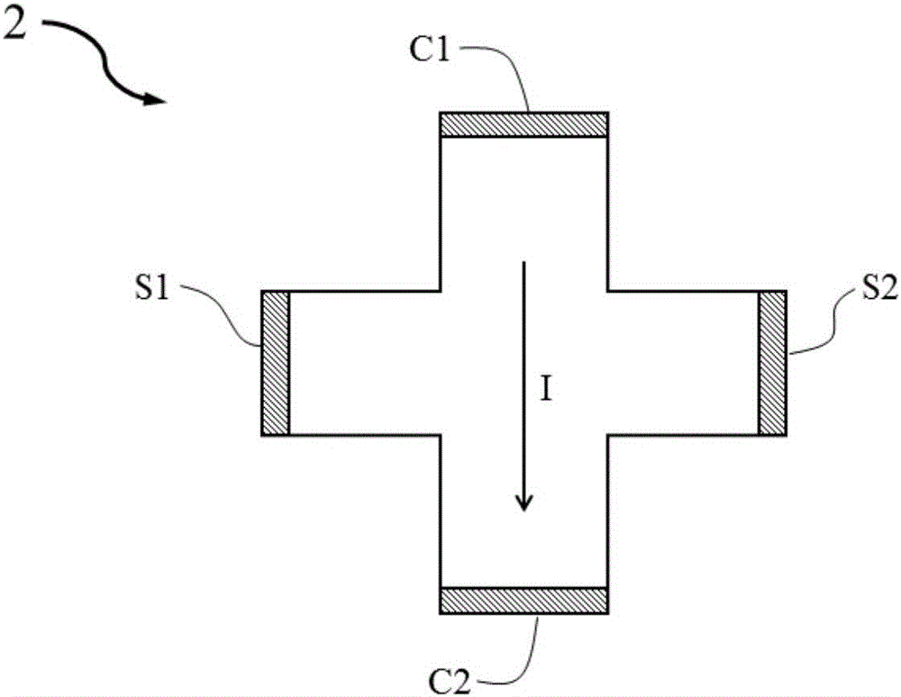
[0007] It can be seen from the above description that the traditional Hall element usually only has a pair of current input terminals C1, C2 and a pair of voltage output terminals S1, S2, resulting in limited testability of the element at the beginning of product design, and due to Semiconductor products require a very long cycle from design, tape-out, to test verification, and product finalization. In addition, the solid structure of the traditional Hall element cannot well correct various parts of the magnetic field required by the user. , which in turn will affect the product design and production cycle, especially if it involves modification of the device structure or circuit, it will have a great impact on the cycle of product introduction to the market, and even affect the normal operation of the product design company

Method used


Image

  • Hall element and Hall element structure
  • Hall element and Hall element structure
  • Hall element and Hall element structure

Examples


Embodiment Construction

[0036] In order to make the content of the present invention clearer and easier to understand, the content of the present invention will be further described below in conjunction with the accompanying drawings. Of course, the present invention is not limited to the following specific embodiments, and general replacements known to those skilled in the art also fall within the protection scope of the present invention.

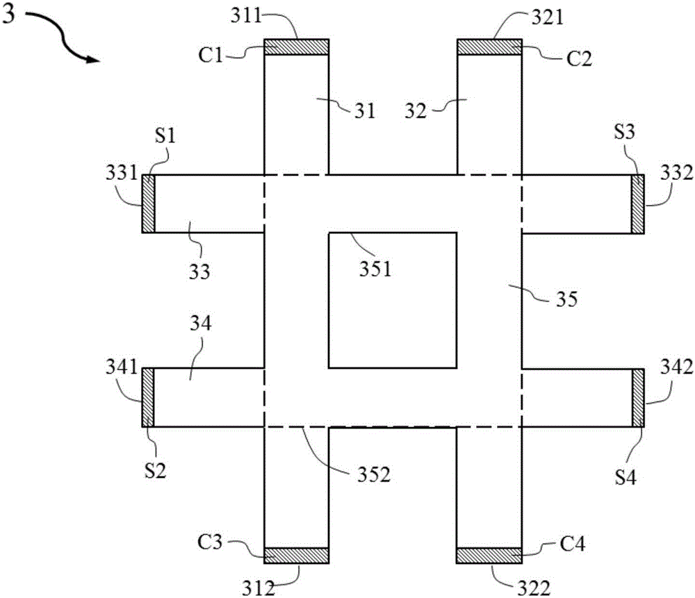
[0037] It should be noted that, for the well-shaped Hall element in the embodiment of the present invention, the two ends in the up and down directions can be used as current input terminals, and the two ends in the left and right directions can be used as Hall voltage output terminals; the two ends in the left and right directions can also be used as The current input terminal and the two ends in the up and down direction are used as the Hall voltage output terminal. And the well-shaped Hall element can have two sets of current input ends in one direction, or a...


PUM


Abstract

The invention provides a Hall element and a Hall element structure. The Hall element includes a square-shaped magnetic sensing part, two pairs of current input and output ends and two pairs of voltage input and output ends; the square-shaped structure includes a rectangular ring part, An outer ring part located at the periphery of the rectangular ring part and an inner ring part surrounded by the rectangular ring part; when there is a magnetic field perpendicular to and / or parallel to the plane where the well-shaped magnetic sensing part is located, acting on the well-shaped magnetic sensing part At this time, the control current is input through at least one pair of the current input and output terminals, and at least one pair of voltage input and output terminals is detected to obtain the corresponding Hall voltage value. The Hall element in the invention can increase the flexibility of product testing and facilitate users to correct the magnetic field.

Description

technical field [0001] The invention belongs to the technical field of semiconductor manufacturing and relates to a Hall element, in particular to a Hall element structure using a cross-shaped magnetic sensing part. Background technique [0002] The Hall sensor is the most commonly used magnetic sensor. Due to its advantages of simple process, low cost, and easy implementation of system-on-chip, it has been widely used in the fields of industrial control, intelligent instrumentation, and consumer electronics. The Hall sensor uses the principle of the Hall effect. When the charged particles move in a magnetic field, they will be affected by the Lorentz force, which will deflect the charged particles and generate an electromotive force perpendicular to the direction of their motion, that is, the Hall voltage. . The shape of an integrated Hall sensor unit is similar to a diffused resistor, except that in order to measure the Hall voltage, it has two more contact holes at right...

Claims


Application Information

Patent Timeline
Patent Type & Authority Patents(China)
IPC IPC(8): G01D5/14H01L43/06H10N52/00
Inventor 王勇赵宇航张剑云张卫
Owner SHANGHAI INTEGRATED CIRCUIT RES & DEV CENT
Learn More