Chip attaching device and method

A chip mounting and chip technology, which is applied in the field of semiconductor packaging, can solve problems such as reducing bonding efficiency and precision, and difficulty in meeting high-efficiency and high-precision requirements of chips, and achieves dispensing, shortening chip transmission strokes, and high-speed and high-precision bonding. The effect of pretending

Inactive Publication Date: 2018-06-12
CETC BEIJING ELECTRONICS EQUIP
View PDF10 Cites 34 Cited by
  • Summary
  • Abstract
  • Description
  • Claims
  • Application Information

AI Technical Summary

Problems solved by technology

[0003] The chip bonding machine determines the accuracy, efficiency and reliability of the chip bonding process. It is the key equipment of the advanced packaging process. The chip bonding machine is a high-speed and high-precision equipment. With the further improvement of semiconductor production efficiency, in order to reduce production costs , the size of the wafer and the bonding base material are developing towards a larger size, the distance from picking up the chip on the wafer to the bonding position of the substrate is increasing, and the general substrate alignment camera is installed on the moving bonding head , greatly reduces the bonding efficiency and precision, and it is difficult to meet the high efficiency and high precision requirements of chip packaging

Method used


Image

  • Chip attaching device and method
  • Chip attaching device and method
  • Chip attaching device and method

Examples


Embodiment Construction

[0073] In order to make the purpose, technical solutions and advantages of the embodiments of the present invention more clear, the following will clearly and completely describe the technical solutions of the embodiments of the present invention in conjunction with the drawings of the embodiments of the present invention. Apparently, the described embodiments are some, not all, embodiments of the present invention. All other embodiments obtained by those skilled in the art based on the described embodiments of the present invention belong to the protection scope of the present invention.

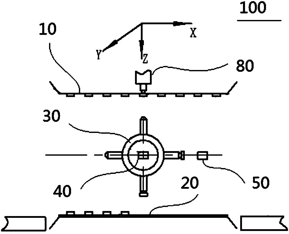
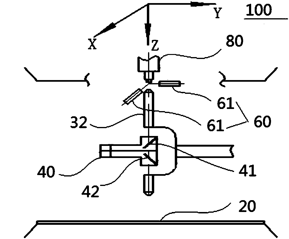
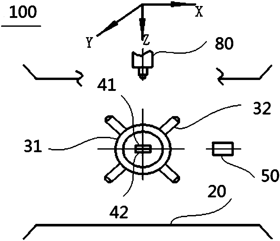
[0074] The chip mounting apparatus 100 according to the embodiment of the present invention will be described in detail below with reference to the accompanying drawings.

[0075] Such as Figure 1 to Figure 7 As shown, the chip mounting apparatus 100 according to the embodiment of the present invention includes a wafer stage 10 , a base material stage 20 , a rotary pick-and-place mechanis...


PUM


Abstract

The invention provides a chip attaching device and method. The device comprises a wafer table, a basic material table, a rotary picking and placing mechanism and a vision mechanism. The wafer table can move in the plane where the wafer table is located; the basic material table is parallel to the wafer table and opposite to the wafer table, and can move in the plane where the basic material tableis located; the rotary picking and placing mechanism is arranged between the wafer table and the basic material table, and provided with a movable bonding portion, wherein the bonding portion can pickup a chip and attach the chip to an attaching position; the vision mechanism is arranged between the wafer table and the basic material table and matched with the rotary picking and placing mechanismto recognize the position of the chip and the attaching position. The method includes the steps that the positions of corresponding parts and components of the chip attaching device are calibrated; the chip is placed at the corresponding position of the attaching device, and position data of the chip is obtained and corrected; the chip is picked up, and the position and the angle data of the picked chip are obtained; the position, for attaching the chip, of a basic material and the angle data of the chip are obtained, the deviation of the chip is calculated and corrected in combination with the position and the angle data of the picked chip, and the chip is attached to the attaching position. With the device and the method, attaching efficiency and accuracy are higher.

Description

technical field [0001] The invention relates to the field of semiconductor packaging, in particular to a chip mounting device and method. Background technique [0002] With the rapid development of integrated circuit advanced packaging technology, the high-speed and high-precision chip mounting process has higher and higher requirements for packaging equipment. Advanced packaging technology integrates semiconductor packaging and assembly technology to reduce product prices, improve performance, increase density and reduce product size, which makes the market demand for high-speed and high-precision chip semiconductor packaging is growing rapidly. The chip bonding process mainly includes chip-to-chip, chip-to-substrate and chip-to-panel packaging technologies. During the chip-to-panel chip mounting process, in order to ensure the mounting quality and accuracy, the panel needs to rise to the temperature required for mounting. Then proceed to the placement process. [0003] T...

Claims


Application Information

Patent Timeline
Patent Type & Authority Applications(China)
IPC IPC(8): H01L21/67
CPCH01L21/67144
Inventor 叶乐志王军帅郎平徐品烈崔洁霍杰周启舟
Owner CETC BEIJING ELECTRONICS EQUIP
Why Eureka
Try Eureka