Display substrate, manufacturing method, display device and fingerprint identification method

A fingerprint recognition and display substrate technology, applied in character and pattern recognition, acquisition/organization of fingerprints/palmprints, matching and classification, etc., can solve the problems of unfavorable narrow-frame products such as thinning, saving space and improving screen ratio Effect

Active Publication Date: 2018-06-15
BOE TECH GRP CO LTD
View PDF20 Cites 9 Cited by
  • Summary
  • Abstract
  • Description
  • Claims
  • Application Information

AI Technical Summary

Problems solved by technology

[0003] In view of this, the present invention provides a display substrate and its manufacturing method, a display device and a fingerprint identification method, which are used to solve the problem that the existing display device needs to reserve a separate position and space for the fingerprint identification module, which is not conducive to narrow borders and Problems in the realization of thinner and lighter products

Method used


Image

  • Display substrate, manufacturing method, display device and fingerprint identification method
  • Display substrate, manufacturing method, display device and fingerprint identification method
  • Display substrate, manufacturing method, display device and fingerprint identification method

Examples


Embodiment Construction

[0035] In order to make the purpose, technical solutions and advantages of the embodiments of the present invention more clear, the following will clearly and completely describe the technical solutions of the embodiments of the present invention in conjunction with the drawings of the embodiments of the present invention. Apparently, the described embodiments are some, not all, embodiments of the present invention. All other embodiments obtained by those skilled in the art based on the described embodiments of the present invention belong to the protection scope of the present invention.

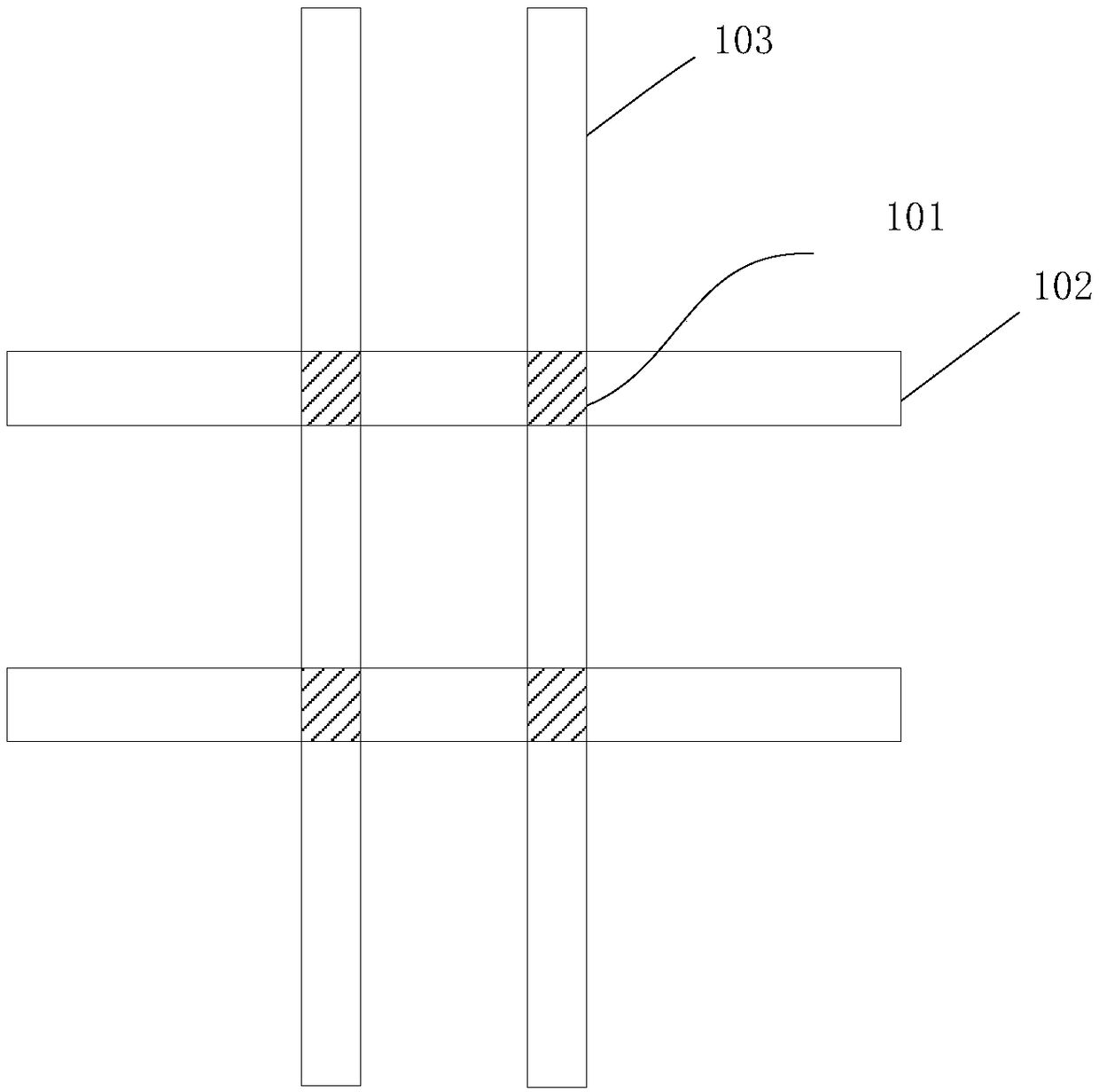
[0036] In order to solve the problem that the existing display device needs to reserve a separate position and space for the fingerprint identification module, which is not conducive to the realization of narrow borders and thinner products, such as figure 1 As shown, the present invention provides a display substrate, including a fingerprint identification module, the fingerprint identific...


PUM


Abstract

The invention provides a display substrate, a manufacturing method thereof, a display device, and a fingerprint identification method. The display substrate comprises a fingerprint recognition moduleset; the fingerprint recognition module set is disposed in a display area of the display substrate; and the fingerprint recognition module set includes a plurality of fingerprint recognition sensors distributed in an arrayed manner, a plurality of scanning lines and a plurality of detection line, wherein the scanning lines are in one-to-one correspondence connection with various rows of fingerprint identification sensors, and the detection lines are in one-to-one correspondence connection with various columns of fingerprint identification sensors, or the scanning lines are in one-to-one correspondence connection with various columns of fingerprint identification sensors, and the detection lines are in one-to-one correspondence connection with various rows of fingerprint identification sensors. With the display substrate, manufacturing method, display device and fingerprint identification method of the invention adopted, fingerprint recognition can be performed in any display area of the display substrate as required, so that the experience of fingerprint recognition can be improved; and no separate positions and spaces need to be reserved for the fingerprint recognition module set,and therefore, the space of a display device provided with the display substrate can be saved, and the realization of narrow-border, thin and light products can be facilitated.

Description

technical field [0001] The invention relates to the technical field of fingerprint identification, in particular to a display substrate and a manufacturing method thereof, a display device and a fingerprint identification method. Background technique [0002] Fingerprint, due to its lifelong invariance, uniqueness and convenience, has almost become synonymous with biometric identification. At present, more and more display devices, especially mobile display devices (such as mobile phones, tablet computers, etc.) are equipped with a fingerprint recognition function. In the existing display device, it is necessary to reserve a separate position and space for the fingerprint identification module on the front or back of the display device, which is not conducive to the realization of narrow borders and thinner products. Contents of the invention [0003] In view of this, the present invention provides a display substrate and its manufacturing method, a display device and a f...

Claims


Application Information

Patent Timeline
Patent Type & Authority Applications(China)
IPC IPC(8): G06K9/00
CPCG06V40/13G01L1/16G06V40/1306H10N30/87H10N30/302G06V40/1365
Inventor 班圣光
Owner BOE TECH GRP CO LTD
Why Eureka
Try Eureka