
Data processing method and device for SSD

A hard disk and data technology, applied in the field of information processing, can solve problems such as complex processing logic and frequent flash memory operations, and achieve the effect of simplifying logic and reducing flash memory operations

Active Publication Date: 2018-07-06
SHENZHEN YILIAN INFORMATION SYST CO LTD
View PDF8 Cites 1 Cited by
  • Summary
  • Abstract
  • Description
  • Claims
  • Application Information

AI Technical Summary

Problems solved by technology

[0006] The embodiment of the present invention provides a data processing method and device for an SSD hard disk, which solves the technical problems of complex logic and frequent flash memory operations in the processing method for writing errors in the SSD hard disk in the prior art

Method used


Image

  • Data processing method and device for SSD
  • Data processing method and device for SSD
  • Data processing method and device for SSD

Examples


Embodiment 1

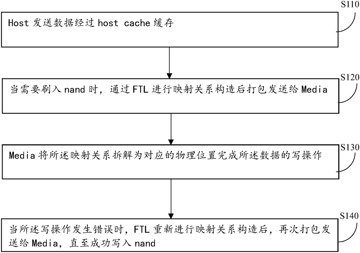
[0039] The embodiment of the present application provides a data processing method of an SSD hard disk, figure 1 It is a schematic flowchart of a data processing method for an SSD hard disk in an embodiment of the present invention. Such as figure 1 As shown, the method includes:

[0040] Step 110: Host sends data through host cache cache;

[0041] Step 120: When the nand needs to be flashed, the mapping relationship is constructed through FTL and then packaged and sent to Media;

[0042] Step 130: Media disassembles the mapping relationship into corresponding physical locations to complete the data writing operation;

[0043] Step 140: When an error occurs in the write operation, after the FTL re-constructs the mapping relationship, it is packaged and sent to Media again until it is successfully written to nand; the re-construction of the mapping relationship of the FTL also includes: the lpn and its The corresponding data is stuffed back into the host cache and processed...

Embodiment 2

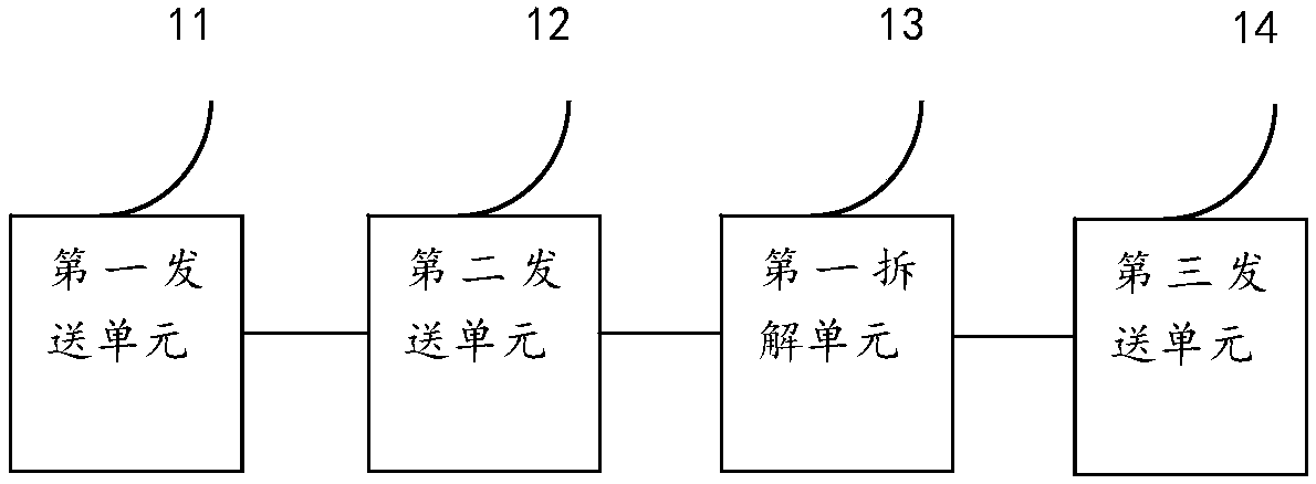
[0049] Based on the same inventive concept as the data processing method of an SSD hard disk in the foregoing embodiments, the present invention also provides a data processing device for an SSD hard disk, such as figure 2 shown, including:

[0050] The first sending unit 11, the first sending unit 11 is used for the Host to send data through the host cache cache;

[0051] The second sending unit 12, the second sending unit 12 is used to pack and send to Media after carrying out the mapping relationship construction by FTL when the nand needs to be brushed in;

[0052] The first disassembly unit 13, the first disassembly unit 13 is used for Media to disassemble the mapping relationship into corresponding physical locations to complete the write operation of the data;

[0053] The third sending unit 14, the third sending unit 14 is used for when an error occurs in the writing operation, after the FTL re-constructs the mapping relationship, it is packaged and sent to the Media...

Embodiment 3

[0060] Based on the same inventive concept as the data processing method of an SSD hard disk in the foregoing embodiments, the present invention also provides a data processing device for an SSD hard disk, on which a computer program is stored, and when the program is executed by a processor, the aforementioned A step in any method of a data processing method for an SSD hard disk.

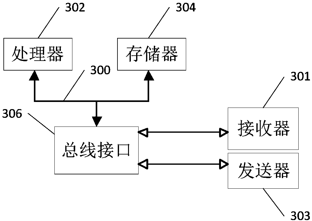
[0061] Among them, in image 3 In, bus architecture (represented by bus 300), bus 300 may include any number of interconnected buses and bridges, bus 300 will include one or more processors represented by processor 302 and various types of memory represented by memory 304 circuits linked together. The bus 300 may also link together various other circuits, such as peripherals, voltage regulators, and power management circuits, etc., which are well known in the art and thus will not be further described herein. The bus interface 306 provides an interface between the bus 300 and the receiver 301 and...


PUM


Abstract

The invention provides a data processing method and device for an SSD and relates to the technical field of information processing. The method includes the steps that data is sent through a host and cached through a host cache; when nand needs to be written in, a mapping relationship is constructed through an FTL and then packed and sent to Media; Media disassembles the mapping relationship into acorresponding physical location to complete a write operation of the data; when the write operation goes wrong, the FTL re-constructs the mapping relationship and then packs and sends the mapping relationship to Media again till nand is successfully written in. The technical effects of simplifying logic and reducing flash memory operations are achieved.

Description

technical field [0001] The invention relates to the technical field of information processing, in particular to a data processing method and device for an SSD hard disk. Background technique [0002] SSD hard drives are fast due to their high write speed. Using flash memory as the storage medium, the reading speed is faster than that of mechanical hard disks, so solid-state hard disks can be widely used in military, vehicle, industrial, medical, aviation and other fields. [0003] In the prior art, when a write error occurs in the SSD hard disk, the write command needs to be resent to the media side for rewriting, so as to ensure that the data can be correctly written to the flash memory of the computer at last, so that the data will not be lost. [0004] However, in the process of realizing the technical solution of the present invention, the inventor of the present application found that the above-mentioned prior art has at least the following technical problems: [0005...

Claims


Application Information

Patent Timeline
IPC IPC(8): G06F3/06
CPCG06F3/0613G06F3/0629G06F3/0656G06F3/0679
Inventor 肖蔓君黄华坤成威
Owner SHENZHEN YILIAN INFORMATION SYST CO LTD
Learn More