Data erasing method and system based on NorFlash chip

A data writing and data technology, applied in memory systems, electrical digital data processing, instruments, etc., can solve the problems of frequent erasing and writing of a certain sector, long time consumption, violations, etc.

Active Publication Date: 2018-07-13
ZHENGZHOU YUNHAI INFORMATION TECH CO LTD
View PDF6 Cites 4 Cited by
  • Summary
  • Abstract
  • Description
  • Claims
  • Application Information

AI Technical Summary

Problems solved by technology

[0004] In the prior art, the data erasing and writing of the NorFlash chip is performed by recording the sector erasing time stamp to realize the equalization of each sector, but this method is very easy to cause the sector The inaccuracy of the erasing and writing time stamps recorded in the internal memory makes the erasing and writing of a certain sector too frequent when the back-calibration span is relatively large, which violates the original intention of sector-balanced erasing. Each sector time stamp needs to be erased and written to each sector, which takes a long time. At this time, once the system is abnormally powered off, it is very easy to cause flash data loss.

Method used


Image

  • Data erasing method and system based on NorFlash chip
  • Data erasing method and system based on NorFlash chip
  • Data erasing method and system based on NorFlash chip

Examples


Embodiment Construction

[0053] In order to make the purposes, technical solutions and advantages of the embodiments of the present application clearer, the technical solutions in the embodiments of the present application will be clearly and completely described below in conjunction with the drawings in the embodiments of the present application. Obviously, the described embodiments It is a part of the embodiments of this application, not all of them. Based on the embodiments in this application, all other embodiments obtained by persons of ordinary skill in the art without making creative efforts belong to the scope of protection of this application.

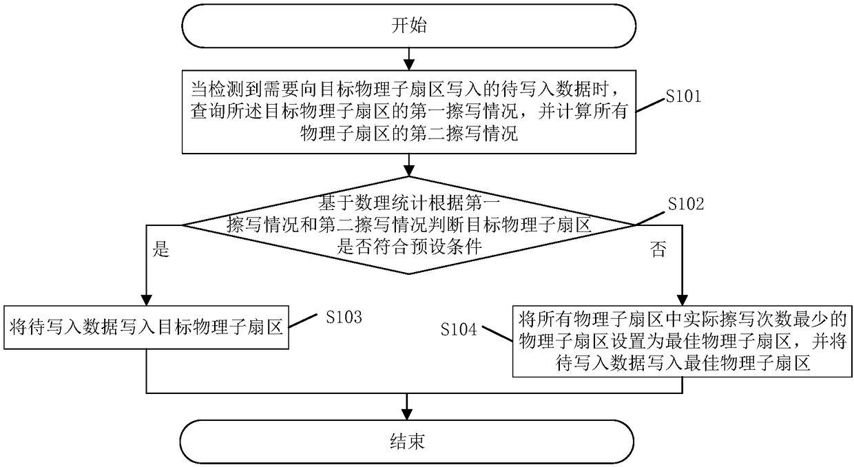
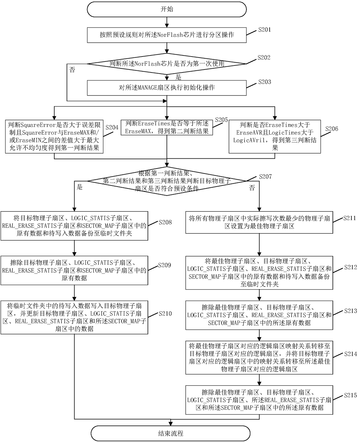
[0054] see below figure 1 , figure 1 It is a flow chart of a method for erasing and writing data based on a NorFlash chip provided by the embodiment of the present application.

[0055] Specific steps can include:

[0056] S101: When the data to be written that needs to be written to the target physical sub-sector is detected, query the first erasi...


PUM


Abstract

The invention discloses a data erasing method based on a Norflash chip. The data erasing method comprises the steps of when it is detected that data to be written needs to be written in a target physical subsector, inquiring first erasing conditions of the target physical subsector and calculating second erasing conditions of all physical subsectors; based on mathematical statistics and accordingto the first erasing conditions and the second erasing conditions, judging whether the target physical subsector satisfies a preset condition or not; if yes, writing the data to be written in the target physical subsector; if not, setting the physical subsector with the smallest actual erasing frequency in all the physical subsectors as an optimal physical subsector and writing the data to be written in the optimal physical subsector. By means of the method, balanced erasing of all the sectors in the Norflash chip can be achieved, and the service life of the NorFlash chip is prolonged. The invention further discloses a data erasing system based on the NorFlash chip. The data erasing system has the advantages.

Description

technical field [0001] The invention relates to the field of data storage, in particular to a method and system for erasing and writing data based on a NorFlash chip. Background technique [0002] Because the NorFlash chip allows applications to run directly on-chip, has higher transmission efficiency and cost-effectiveness, and has the characteristics of not losing data when power is turned off, many embedded products use the NorFlash chip as a storage device for applications and important data. [0003] According to the principle of flash programming, only 1 can be written as 0, but 0 cannot be written as 1. Therefore, before flash programming, the data of the corresponding storage unit needs to be erased first. At present, the erasing method provided by the flash chip includes sector There are two types of erase (Sector Erase) and chip erase (Chip Erase). Therefore, before writing data to a flash storage unit, the sector where the storage unit is located must be erased fi...

Claims


Application Information

Patent Timeline
Patent Type & Authority Applications(China)
IPC IPC(8): G06F12/02
CPCG06F12/0246G06F2212/7211
Inventor 候志立
Owner ZHENGZHOU YUNHAI INFORMATION TECH CO LTD
Why Eureka
Try Eureka