A display panel, its detection method, its manufacturing method and display device

A display panel and detection circuit technology, applied in semiconductor devices, electrical components, circuits, etc., can solve the problems of occupied pixel aperture ratio and low resolution of display panel

Active Publication Date: 2020-11-03
BOE TECH GRP CO LTD +1
View PDF5 Cites 0 Cited by
  • Summary
  • Abstract
  • Description
  • Claims
  • Application Information

AI Technical Summary

Problems solved by technology

[0005] Embodiments of the present invention provide a display panel, a manufacturing method thereof, and a display device to solve the problem in the prior art that the resolution of the display panel is low due to the aperture ratio of pixels occupied by the infrared light-emitting part and the infrared photosensitive detection unit

Method used


Image

  • A display panel, its detection method, its manufacturing method and display device
  • A display panel, its detection method, its manufacturing method and display device
  • A display panel, its detection method, its manufacturing method and display device

Examples


Embodiment Construction

[0051] In view of the problem of low resolution of the display panel due to the aperture ratio of the pixels occupied by the infrared light-emitting part and the infrared photosensitive detection unit in the prior art, embodiments of the present invention provide a display panel, a manufacturing method thereof, and a display device.

[0052] In the following, specific implementations of the display panel, the manufacturing method thereof, and the display device provided by the embodiments of the present invention will be described in detail with reference to the accompanying drawings. The thickness and shape of each film layer in the drawings do not reflect the true ratio, and the purpose is only to illustrate the content of the present invention schematically.

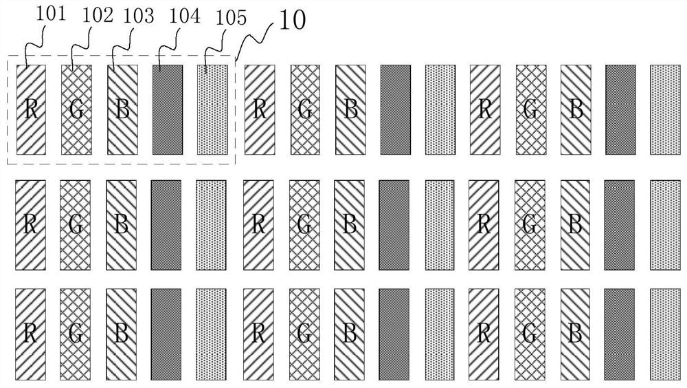
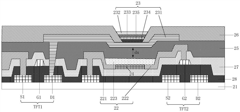
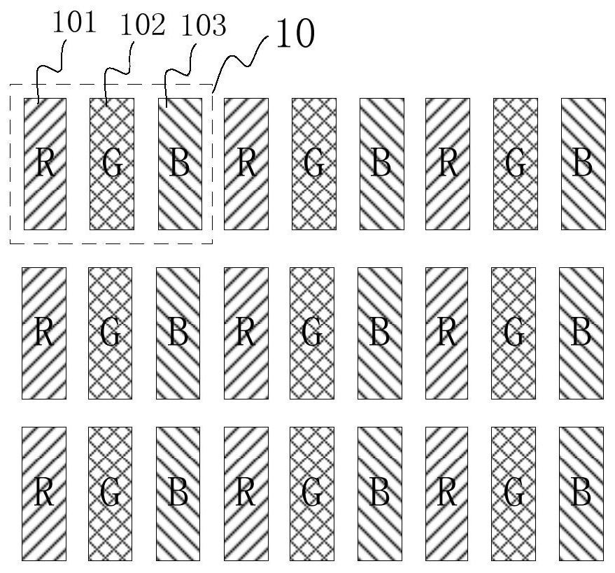
[0053] In the first aspect, an embodiment of the present invention provides a display panel, such as figure 2 with image 3 As shown, it includes: a base substrate 21, a plurality of pixels 10 arranged in an array on the b...


PUM


Abstract

The invention discloses a display panel, its manufacturing method and a display device. The display panel includes: a base substrate, a plurality of pixels arranged in an array on the base substrate, and a detection circuit; wherein each pixel It includes a plurality of sub-pixels; the sub-pixels include: an infrared detection unit located on the base substrate, and a light-emitting unit located on the side of the infrared detection unit away from the base substrate; the light-emitting unit includes: a first electrode located on the base substrate, The second electrode located on the side of the first electrode away from the base substrate, and the display light-emitting part and the infrared light-emitting part stacked between the first electrode and the second electrode; the detection circuit is electrically connected to each infrared detection unit for The touch position is judged according to the photocurrent signal of each infrared detection unit. In the display panel provided by the embodiment of the present invention, the infrared detection unit and the infrared light emitting part do not occupy the aperture ratio of the pixel, which improves the resolution of the display screen.

Description

Technical field [0001] The present invention relates to the field of display technology, in particular to a display panel, a manufacturing method thereof, and a display device. Background technique [0002] Organic Light-Emitting Diode (OLED) display panels have excellent characteristics such as high contrast, wide color gamut, fast response speed, and flexibility, which arouse the enthusiasm for commercial production in the flat panel industry and become the future display technology Competitor with the most development potential. Among them, Active-matrix organic light emitting diode (AMOLED) display panels have been widely used. [0003] With the gradual maturity of organic electroluminescence (OLED) display panel technology, and the simultaneous development of in-cell technology that integrates the touch screen sensing layer with AMOLED, AMOLED screens based on on-cell touch technology have been commercialized It has begun to be used in public services and personal entertainm...

Claims


Application Information

Patent Timeline
Patent Type & Authority Patents(China)
IPC IPC(8): H01L27/32
CPCH10K59/40H10K59/12H10K59/1201
Inventor 朱儒晖邹清华王玉姚固曾苏伟潘杰
Owner BOE TECH GRP CO LTD
Why Eureka
Try Eureka