CIS-based squint imaging device and method

An imaging device and angled technology, applied in the imaging field, can solve the problems of low work efficiency, inability to guarantee the image shooting effect, easy occurrence of overexposure, reflection, etc., to ensure the quality of image acquisition and prevent overexposure.

Active Publication Date: 2018-08-03
杭州创恒电子技术开发有限公司
View PDF6 Cites 0 Cited by
  • Summary
  • Abstract
  • Description
  • Claims
  • Application Information

AI Technical Summary

Problems solved by technology

However, it still has the following disadvantages: when the CIS sensor takes light, it is still perpendicular to the surface of the measured object, which is prone to overexposure and reflection, and cannot solve the problem of oblique imaging of smooth objects; and th

Method used


Image

  • CIS-based squint imaging device and method
  • CIS-based squint imaging device and method

Examples


Embodiment 1

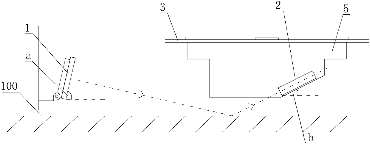
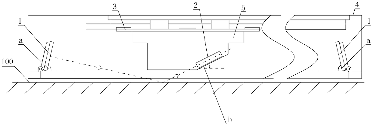
[0025] Such as Figure 1-2 As shown, a squint imaging device based on CIS includes a light source 1 , a CIS sensor 2 and an imaging circuit 3 . The light source 1 irradiates light on the surface 100 of the measured object, the CIS sensor 2 can receive the light reflected by the light source 1 from the surface 100 of the measured object, and the imaging circuit 3 is connected to the CIS sensor 2 . The light source 1, the CIS sensor 2 and the imaging circuit 3 can adopt existing structures. And the light intensity of the light source 1 can be adjusted according to the shooting scene.

[0026] Among them, the CIS sensor 2 is a contact image sensor (Contact Image Sensor, CIS), which closely arranges the photosensitive units to directly collect the light information reflected by the scanned footprints. The CIS consists of a micro self-focusing rod lens array (RodLens array), a photoelectric sensor Array (CMOS image sensor array) and its circuit board, protective glass, interface,...

Embodiment 2

[0034] This embodiment is an improvement made on the basis of Embodiment 1, and this Embodiment 2 is the usage method of the squint imaging device based on CIS in Embodiment 1.

[0035] A squint imaging method based on CIS, comprising the following steps: a light source 1 emits light to the surface 100 of the measured object at an angle a to the surface 100 of the measured object, and then the CIS sensor 2 receives the measured object at an angle b to the surface 100 of the measured object The light reflected by the object surface 100, and then the CIS sensor 2 transmits the reflected light to the imaging circuit 3; the value range of a is 80°

[0036] In order to improve the flexibility of use, the light source 1 can be rotated along the body 4 to adjust the angle a, the CIS sensor 2 is arranged on the lens 5, and the lens 5 moves along the body 4 through a sliding device. Then adjust the light-taking position.

[0037] In order ...


PUM


Abstract

The invention relates to the technical field of imaging, and particularly discloses a CIS-based squint imaging device and method. The device comprises a light source irradiated on a surface of an object to be tested, a CIS sensor capable of receiving light reflected by the light source from the surface of the object to be tested, and an imaging circuit connected to the CIS sensor, wherein the light source forms an angle a with the surface of the object to be tested; the CIS sensor forms an angle b with the surface of the object to be tested to receive the light reflected by the light source from the surface of the object to be tested; and the value range of a is that a is greater than 80 degrees and less than 90 degrees, and the value range of b is that b is greater than 20 degrees and less than 30 degrees. According to the scheme of the invention, the image collection quality can be ensured, the phenomena of overexposure and light reflection can be effectively prevented, the concave and convex effect on an image can be clearly identified by only taking one photo, and the working efficiency can be improved.

Description

technical field [0001] The invention relates to the field of imaging technology, in particular to a CIS-based squint imaging device and method. Background technique [0002] At present, most of the imaging methods on the market are top-down imaging and squint imaging. The top-down imaging uses a low-side light for initial footprint visualization, and uses CMOS or linear CCD top-down imaging. This method will miss many footprint details, and many difficult footprints are Imaging is not possible; strabismus imaging uses CMOS or linear CCD imaging, this method the overall picture is very blurry, and many footprint details of luminous objects such as tiles cannot be displayed. [0003] In order to solve the above problems, an invention patent application with the application number 201010533349.3 and titled "A Multi-angle Optical Feature Detection Method and Device" appeared. This application introduced a CIS sensor and simultaneously acquired the first image of the detection ar...

Claims


Application Information

Patent Timeline
IPC IPC(8): H04N5/225G03B17/17
CPCG03B17/17H04N23/50H04N23/54
Inventor 王亮
Owner 杭州创恒电子技术开发有限公司
Why Eureka
Try Eureka