Array substrate and preparation method thereof, and display device

An array substrate, source-drain technology, applied in semiconductor/solid-state device manufacturing, electrical components, electrical solid-state devices, etc., can solve problems such as poor compatibility, increase pixel capacitance, improve production yield, and improve product performance. Effect of Voltage Compensation Capability

Active Publication Date: 2018-08-07
BOE TECH GRP CO LTD
View PDF4 Cites 29 Cited by
  • Summary
  • Abstract
  • Description
  • Claims
  • Application Information

AI Technical Summary

Problems solved by technology

The inventors found that this is mainly due to the poor compatibility of the fabrication pro

Method used


Image

  • Array substrate and preparation method thereof, and display device
  • Array substrate and preparation method thereof, and display device
  • Array substrate and preparation method thereof, and display device

Examples


Embodiment Construction

[0035] Embodiments of the present invention are described in detail below, examples of which are shown in the drawings, wherein the same or similar reference numerals designate the same or similar elements or elements having the same or similar functions throughout. The embodiments described below by referring to the figures are exemplary only for explaining the present invention and should not be construed as limiting the present invention.

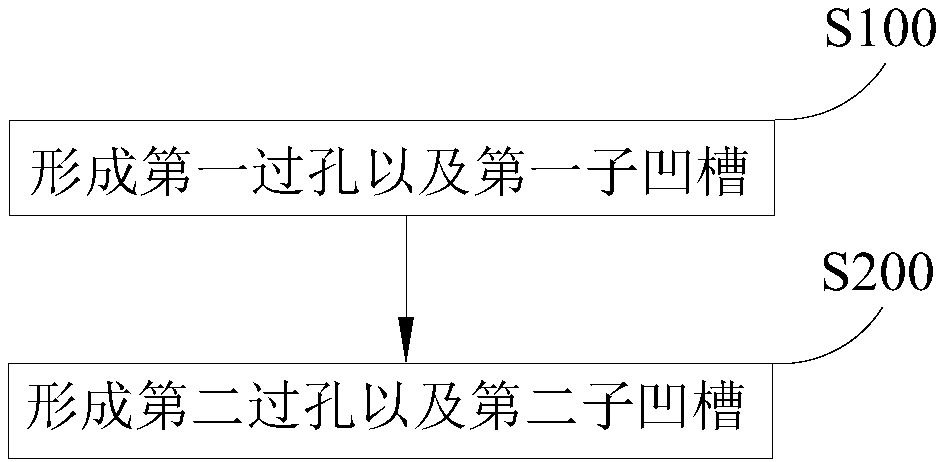
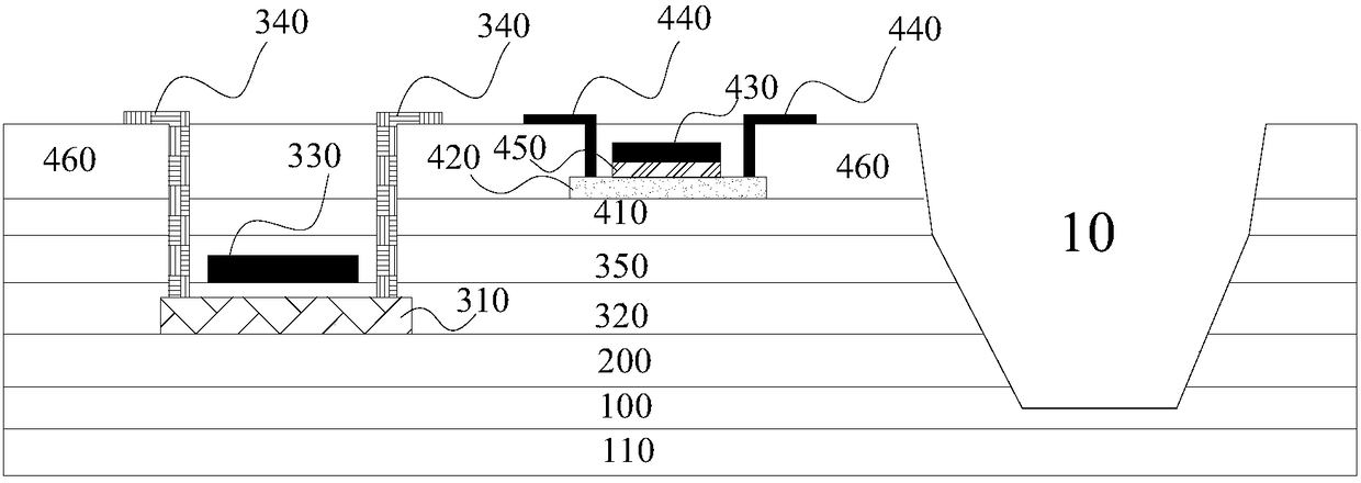
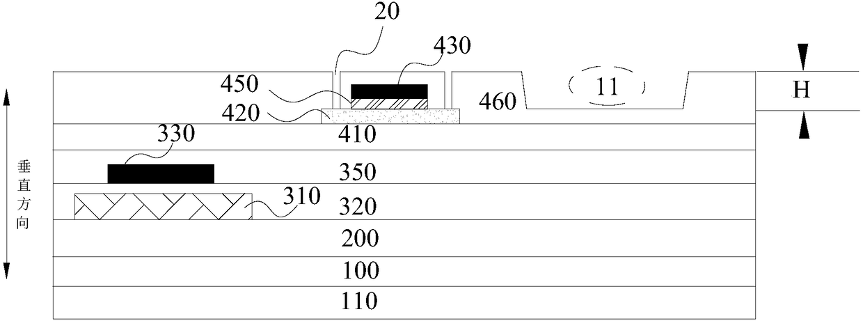
[0036] In one aspect of the invention, the invention provides a method for preparing an array substrate. Specifically, the array substrate prepared by this method may be an array substrate having a plurality of thin film transistors. More specifically, the method can be used to prepare an array substrate with different depths of active layers of multiple thin film transistors. For example, according to a specific embodiment of the present invention, the array substrate may include an array substrate of low-temperature polysilicon thin f...


PUM


Abstract

The invention discloses an array substrate and a preparation method thereof, and a display device. A base of the array substrate is provided with a first film transistor and a second film transistor and a groove arranged in a wiring region, wherein the groove comprises a first sub groove and a second sub groove. The method comprises steps that a first through hole and the first sub groove are formed through employing the one-time picture composition process; the second through hole and the second sub groove are formed through employing the one-time picture composition process. The method is advantaged in that a problem of active layer over-etching due to difference in depth of the two through holes when the two through holes are formed synchronously is solved, and prolongation of the production process is avoided.

Description

technical field [0001] The present invention relates to the field of display technology, in particular, to an array substrate, a manufacturing method thereof, and a display device. Background technique [0002] At present, with the development of semiconductor manufacturing technology and display technology, the competition in the display field is becoming increasingly fierce, and the performance requirements of users for display devices are also increasing. Display devices with high definition, high contrast and high aperture ratio are becoming more and more popular among users. Welcome. In addition, new display devices such as flexible screens and full-screen borderless display products also show huge market prospects. Array substrates, such as the backplane of organic light-emitting display devices, are important components that affect the performance of display devices. Thin film transistors are important switch control devices in array substrates. In recent years, low...

Claims


Application Information

Patent Timeline
IPC IPC(8): H01L21/77H01L27/32
CPCH01L21/77H10K59/12H01L27/1225H01L27/124H01L27/1255H01L27/1259H01L29/66969H01L27/1251H01L29/66757H01L29/78675H01L29/7869H10K59/1213H10K59/1216
Inventor 杨维卢鑫泓
Owner BOE TECH GRP CO LTD
Why Eureka
Try Eureka