Liquid crystal display device

a display device and liquid crystal technology, applied in non-linear optics, instruments, optics, etc., can solve problems such as display quality degradation, and achieve the effects of suppressing problems, increasing pixel capacitance, and suppressing flickering or the lik

Inactive Publication Date: 2015-08-06
SHARP KK
View PDF3 Cites 14 Cited by
  • Summary
  • Abstract
  • Description
  • Claims
  • Application Information

AI Technical Summary

Benefits of technology

[0017]According to the aspect of the invention, it is possible to realize a liquid crystal display device which increases pixel capacitance to suppress flickering or the like while suppressing the occurrence of problems of degradation of light transmittance, color mixing, and the like, and achieves high display quality.

Problems solved by technology

If the pixel capacitance decreases, flickering or crosstalk is likely to occur, causing deterioration of display quality.

Method used


Image

  • Liquid crystal display device
  • Liquid crystal display device
  • Liquid crystal display device

Examples


first embodiment

[0026]Hereinafter, a first embodiment of the invention will be described referring to FIGS. 1 to 5.

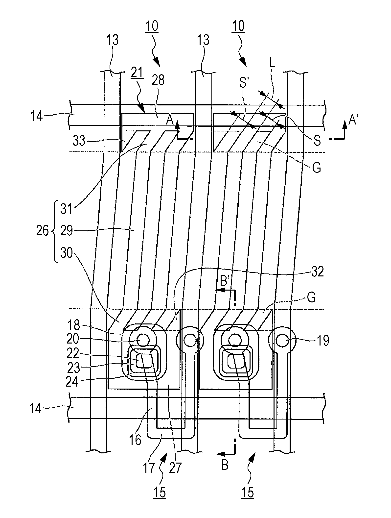
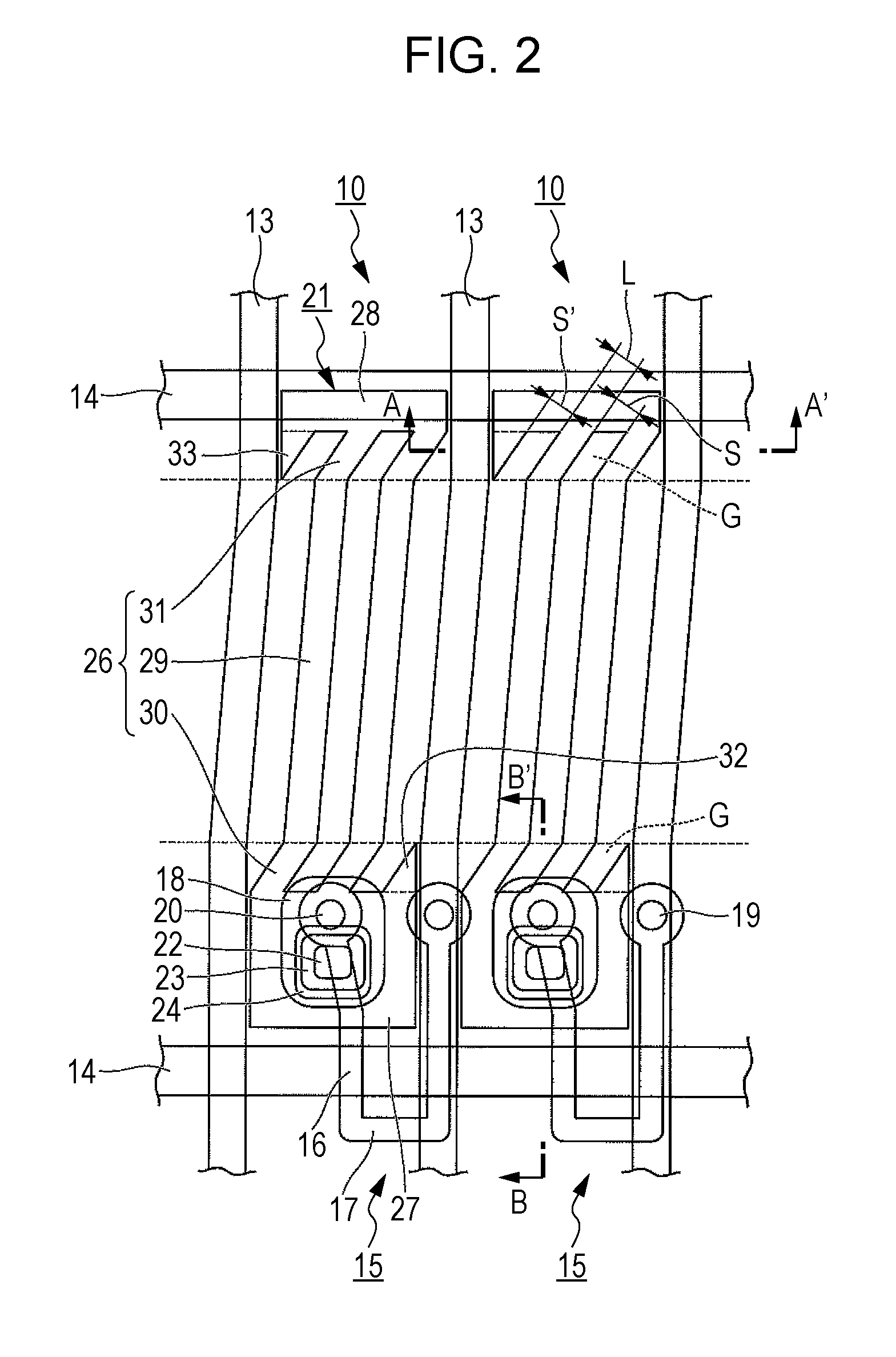
[0027]A liquid crystal display device of this embodiment is a transverse field liquid crystal display device, particularly, an FSS liquid crystal display device which includes a first electrode and a second electrode on one substrate of a pair of substrates with a liquid crystal layer sandwiched therebetween, and drives liquid crystal by an electric field applied between the first electrode and the second electrode.

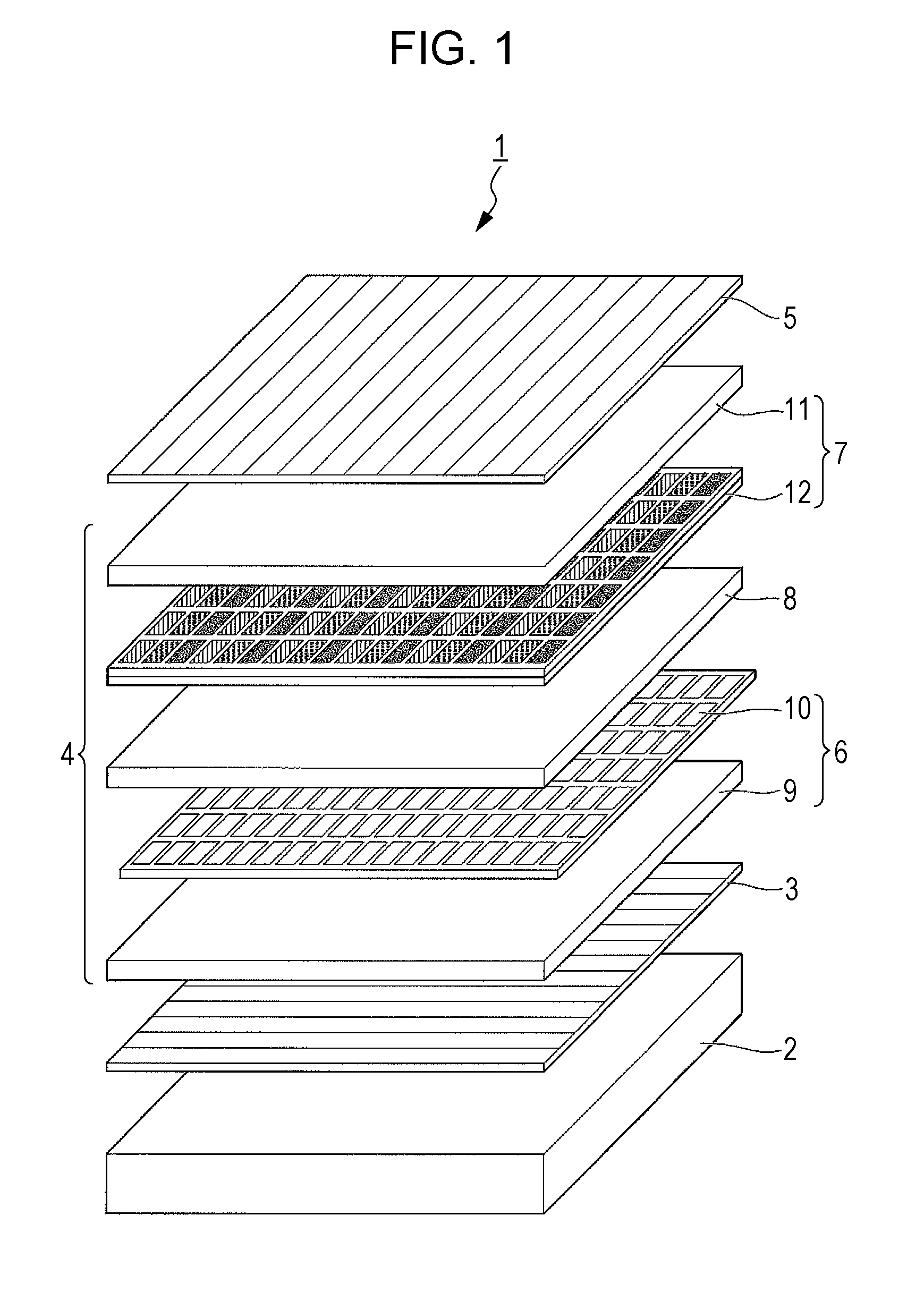
[0028]FIG. 1 is an exploded perspective view showing the schematic configuration of the liquid crystal display device of this embodiment. FIG. 2 is a plan view showing two adjacent pixels of the liquid crystal display device of this embodiment. FIG. 3 is a cross-sectional view taken along the line A-A′ of FIG. 2. FIG. 4 is a cross-sectional view taken along the line B-B′ of FIG. 2.

[0029]In the respective drawings, the scale of the size of each constituent has been adjusted t...

first modification example

[First Modification Example of Pixel Electrode]

[0069]In the foregoing embodiment, although the triangular additional capacitance portions 32 and 33 are provided, the shape of the additional capacitance portion may not be necessarily a triangular shape.

[0070]FIG. 6 is a plan view showing two adjacent pixels of a liquid crystal display device of a first modification example.

[0071]In FIG. 6, the constituents common to FIG. 2 are represented by the same reference numerals, and description thereof will not be repeated.

[0072]In a pixel electrode 50 of this modification example, a rectangular additional capacitance portion 51 is provided in a region along the arrangement direction of a plurality of first bent portions 30. Similarly, a rectangular additional capacitance portion 52 is provided in a region along the arrangement direction of a plurality of second bent portions 31. The additional capacitance portions 51 and 52 are disposed in the light-shielding region G together with the first...

second modification example

[Second Modification Example of Pixel Electrode]

[0074]In the foregoing embodiment, although the entire additional capacitance portions 32 and 33 are disposed in the light-shielding region G, the entire additional capacitance portion may not be necessarily disposed in the light-shielding region.

[0075]FIG. 7 is a plan view showing two adjacent pixels of a liquid crystal display device of a second modification example.

[0076]In FIG. 7, the constituents common to FIG. 2 are represented by the same reference numerals, and description thereof will not be repeated.

[0077]In a pixel electrode 55 of this modification example, a substantially triangular additional capacitance portion 56 is provided in a region along the arrangement direction of a plurality of first bent portions 30. In the additional capacitance portion 56, the side close to the first connection portion 27 is disposed in the light-shielding region G, and the side (the leading end side of the triangle) distant from the first con...


PUM

PropertyMeasurementUnit
widthaaaaaaaaaa
capacitanceaaaaaaaaaa
lengthaaaaaaaaaa

Abstract

A liquid crystal display device includes a TFT array substrate (first substrate), a counter substrate (second substrate), a liquid crystal layer, and a common electrode (first electrode), an insulating film, and pixel electrodes 21 (second electrode) that are provided on the TFT array substrate. Each of the pixel electrodes 21 has a plurality of linear electrodes 26 and a first connection portion 27. Each of the linear electrodes 26 has a main line portion 29 and a first bent portion 30. An additional capacitance portion 32 is provided integrally with the first connection portion 27 in a region along an arrangement direction of a plurality of first bent portions 30.

Description

TECHNICAL FIELD[0001]The present invention relates to a liquid crystal display device.[0002]This application claims priority based on Japanese Patent Application No. 2012-221529, filed on Oct. 3, 2012, the contents of which are incorporated herein by reference.BACKGROUND ART[0003]In a liquid crystal display device, a transverse field system is hitherto known as a system which applies an electric field to a liquid crystal layer. In a transverse field liquid crystal display device, a common electrode and pixel electrodes are provided on one substrate of a pair of substrates with a liquid crystal layer sandwiched therebetween, and an electric field in a substantially transverse direction (a direction substantially parallel to the substrates) relative to the liquid crystal layer is applied to the liquid crystal layer. In this case, since directors of liquid crystal molecules are not erected in a direction perpendicular to the substrates, there is an advantage that a viewing angle is wid...

Claims


Application Information

Patent Timeline
Patent Type & Authority Applications(United States)
IPC IPC(8): G02F1/1362G02F1/1343G02F1/1335G02F1/1368G02F1/1333
CPCG02F1/133345G02F1/133512G02F1/134309G02F2001/134372G02F1/1368G02F2001/13606G02F1/134363G02F1/136286G02F1/1362G02F1/134372G02F1/13606
Inventor KAWASHIMA, YUKIKAISE, YASUYOSHI
Owner SHARP KK
Why Eureka
Try Eureka