Display device, transparent OLED array substrate and manufacturing method of array substrate

A technology of an array substrate and a manufacturing method, which is applied in the display field and can solve problems such as increasing haze, increasing panel transparency, and uneven display brightness

Inactive Publication Date: 2019-03-08
BOE TECH GRP CO LTD
View PDF3 Cites 7 Cited by
  • Summary
  • Abstract
  • Description
  • Claims
  • Application Information

AI Technical Summary

Problems solved by technology

[0003] In the prior art, when increasing the transparency of the panel and improving the display effect, there will be conflicting problems between increasing the transparency of the panel and increasing the

Method used


Image

  • Display device, transparent OLED array substrate and manufacturing method of array substrate
  • Display device, transparent OLED array substrate and manufacturing method of array substrate
  • Display device, transparent OLED array substrate and manufacturing method of array substrate

Examples


Embodiment Construction

[0058] Example embodiments will now be described more fully with reference to the accompanying drawings. Example embodiments may, however, be embodied in many forms and should not be construed as limited to the embodiments set forth herein; rather, these embodiments are provided so that this disclosure will be thorough and complete, and will fully convey the concept of example embodiments to those skilled in the art. The same reference numerals in the drawings denote the same or similar structures, and thus their detailed descriptions will be omitted.

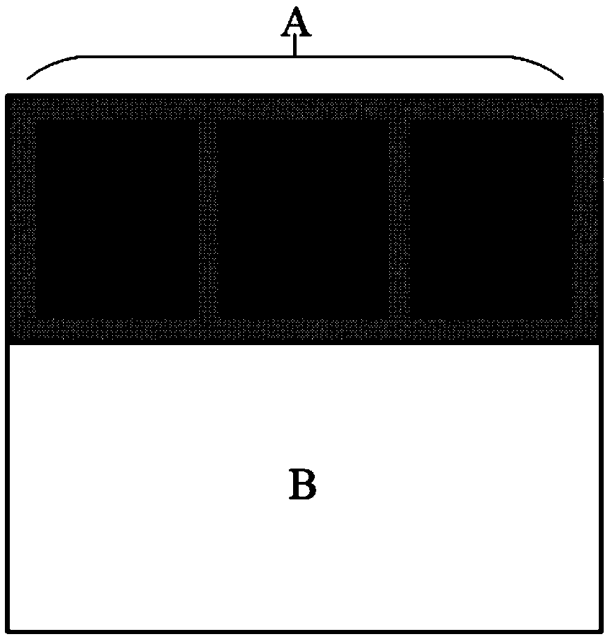
[0059] refer to figure 1 The schematic diagram of area division of the transparent display panel in the related art is shown. The transparent display panel mainly includes pixel unit A and transparent area B. The pixel unit is composed of red, green and blue sub-pixels, which are opaque. When the pixel density, that is, the resolution is constant, in order to increase the transparency of the panel and improve the display effe...


PUM


Abstract

The invention relates to the technical field of display, and provides a transparent OLED array substrate. The transparent OLED array substrate comprises a driver transistor, a metal shading layer, a buffer layer, an active layer, an interlayer dielectric layer and an electrode layer. The metal shading layer comprises a first metal shading layer located at the bottom of the driver transistor and asecond metal shading layer located in a capacitor region and serving as one electrode of a capacitor; the buffer layer is arranged on the metal shading layer; the active layer is arranged on the buffer layer, and comprises a first active layer of the driver transistor and a second active layer arranged opposite to the second metal shading layer; the first active layer and the second active layer are separated; a first capacitor is formed by the second active layer and the second metal shading layer; the interlayer dielectric layer is arranged on the active layer; and the electrode layer is arranged in a region, opposite to the second active layer, of the interlayer dielectric layer, and forms a second capacitor together with the second active layer. The pixel capacitance is increased; thedisplay uniformity is improved; the area of the metal shading layer is reduced; the haze is reduced; and the display effect is improved.

Description

technical field [0001] The present invention relates to the field of display technology, in particular to a transparent OLED array substrate, a manufacturing method of the transparent OLED array substrate and a display device installed with the transparent OLED array substrate. Background technique [0002] With the rapid development of display technology, people have higher and higher requirements for display technology. [0003] In the prior art, when increasing the transparency of the panel and improving the display effect, there will be conflicting problems between increasing the transparency of the panel and increasing the pixel capacitance value to reduce the uneven display brightness; there will also be large reflective shading in the transparent display panel Metal will increase haze, which will reduce the lack of display effect. [0004] Therefore, it is necessary to study a new transparent OLED array substrate, a transparent OLED array substrate, a manufacturing m...

Claims


Application Information

Patent Timeline
IPC IPC(8): H01L27/32H01L27/12H01L29/786H01L21/77
CPCH01L27/1255H01L29/78633H10K59/1213H10K59/1201
Inventor 宋振王国英
Owner BOE TECH GRP CO LTD
Why Eureka
Try Eureka